First prototypes of UVB micro-LEDs presented
The Ferdinand Braun Institute has fabricated micro light-emitting diodes in the UV spectral range. The tiny LEDs can be densely packed to form high-resolution arrays.
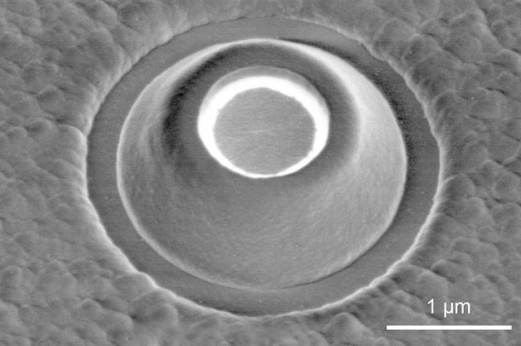
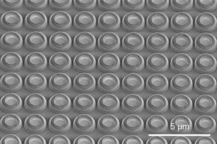
Researchers at the FBH in Berlin have successfully produced the first prototypes of micro-LEDs that emit in the ultraviolet spectral range (UVB). The micro-LEDs with 310 nm emission wavelength feature a small size of the emitting area with diameters down to 1.5 µm. This is hundreds to thousands of times smaller than conventional UV LEDs. The micro-LEDs can be closely packed with pitches down to 2 µm to form a two-dimensional array on a chip, resulting in high-resolution UVB emitting areas.
Used either as single emitter or arranged as a high-density array, UV micro-LEDs can be used in a wide range of applications. This includes sensing technology, curing of polymers and resins, production of semiconductor chips, and optical communication. On FBH’s current chips, all UV micro-LEDs of an array are operated simultaneously. In the next step, the LED pixels are to be individually addressed via a control chip. This will allow to generate and quickly modulate individual illumination patterns, enabling mask-free photolithography, for example. Individual structures can thus be created on semiconductor wafers easily, quickly, and cost-effectively. The capability of high-resolution UV irradiation patterns also opens up new applications in the field of rapid prototyping and fluorescence analysis. In parallel, FBH scientists are already transferring this technology to UVC LEDs, including far-UVC LEDs with extremely short emission wavelengths around 230 nm. Now, the FBH is looking for partners who intend to use UV micro-LEDs in their applications, aiming to jointly advance the technology and fully exploit the potential of the devices.
Highest demands on chip processing technology
Semiconductor layer structures emitting in the ultraviolet spectral range were deposited by means of metal organic vapor phase epitaxy and then patterned using lithographic processes, plasma etching, and deposition methods. Fabricating UV micro-LEDs with small diameters in the range between 1.5 and 50 µm and with a pitch between 2 and 60 µm required a high alignment accuracy, manufacturing precision, and material perfection. This could only be met by using state-of-the-art lithographic processes that were specially designed for this application. Precise alignment of the different process layers to each other (overlay control) with an accuracy of better than 20 nm over the 2-inch LED wafer was needed. Due to the small dimensions of the fabricated UV micro-LEDs – such as diameter, shape, and slope angle of the etched structures – their properties were controlled by means of electron microscopy.
Company
Ferdinand-Braun-Institut, Leibniz-Institut für HöchstfrequenztechnikGustav-Kirchhoff-Str. 4
12489 Berlin
Germany


most read
Sick increases sales in 2025
In the 2025 financial year, the company increased its turnover to 1.85 billion euros, an increase of 6.5% compared to the previous year.
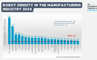
Global robot density: Western Europe leads ahead of North America and Asia
In the EU-27, the robot density is 231, which is above the global average of 132.
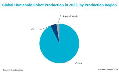
The market for humanoid robots is growing rapidly
Global production of humanoid robots rose to over 20,000 units in 2025, a tenfold increase compared to 2024.

5 robotics trends for 2026
The International Federation of Robotics reports on the five most important trends for the robotics industry in 2026.

TPL Vision joins EMVA
The company is looking forward to working together and sharing knowledge within the industry