Fraunhofer expands Apecs’ possibilities
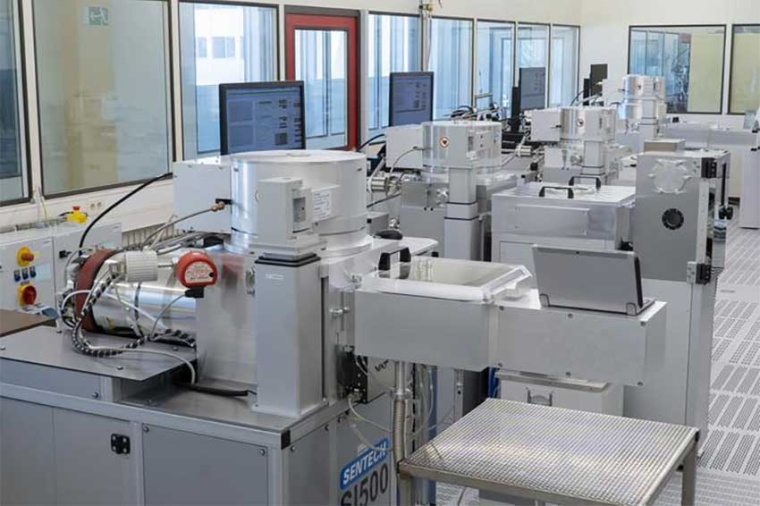
As part of the pilot line, the Fraunhofer Institute for Applied Solid State Physics will continue to expand its semiconductor research infrastructure.
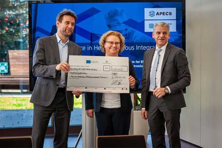
Fraunhofer IAF is expanding its technological capabilities in the field of III-V compound semiconductors, making a valuable contribution to the development of the Advanced Packaging and Heterogeneous Integration for Electronic Components and Systems “Apecs” pilot line within the framework of the EU Chips Act. The Baden-Württemberg Ministry of Economic Affairs, Labor and Tourism is contributing 4.35 million euros to the funding. On 16 December 2024, State Secretary for Economic Affairs Dr Patrick Rapp symbolically handed over a cheque for the funding amount to the institute’s directors. Apecs will further expand the research and development infrastructure across Europe, integrating core technologies, including CMOS and III-V for RF, photonics, and sensors.
Apecs is an important component of the EU Chips Act to drive chiplet innovation and increase research and manufacturing capacity for semiconductors in Europe. The institutes cooperating in the FMD are working closely with other European partners to set up the pilot line and are thus making a significant contribution to strengthening Europe’s technological resilience and thus also increasing global competitiveness in the semiconductor industry.
The pilot line will provide large industrial companies as well as small and medium-sized enterprises (SMEs) and start-ups with low-threshold access to cutting-edge technologies and ensure secure, resilient semiconductor value chains. Apecs is co-funded by Chips Joint Undertaking and by national funding from Austria, Belgium, Finland, France, Germany, Greece, Portugal and Spain under the Chips for Europe initiative. The total funding for the Apecs pilot line amounts to EUR 730 million over four and a half years.
Apecs focuses on the scalable industrial transfer of newly developed innovations in the field of heterointegration, in particular the use of new chiplet technologies, thus building a bridge to application-oriented research. It goes beyond conventional system-in-package (SiP) methods and aims to deliver robust and trustworthy heterogeneous systems that significantly increase the innovative capacity of the European semiconductor industry.
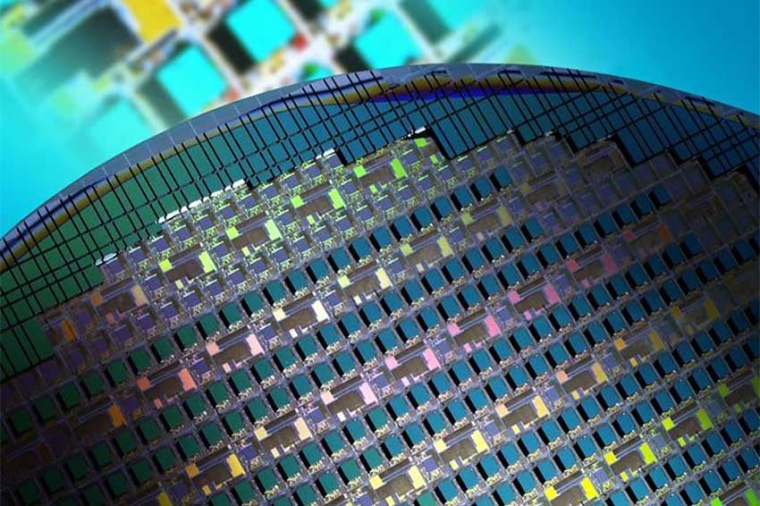
The increasing performance and cost requirements for electronic components mean that conventional semiconductor chips are increasingly reaching their technological limits. The processing of large integrated circuits, as required for comprehensive functionalities, causes high costs, as individual defects have an extremely strong impact on the yield of a single wafer. In addition, chemical and mechanical incompatibilities between different materials and layer structures mean that only a limited number of different technologies can be implemented on a single wafer.
A novel solution for efficiently increasing system functionality is the electrical or optical connection of individual small components (so-called chiplets) on a common substrate (interposer). With the chiplet approach, the individual technologies can each undergo the optimum epitaxy and processing for them and then form a highly functional, flexible and efficient chip-sized system through low-loss integration. This modularization also increases scalability, simplifies chip design and shortens the time to market for innovations.
Link: APECS Pilot Line, Fraunhofer Institute for Photonic Microsystems IPMS, Dresden, Germany
Company
Fraunhofer Institute for Applied Solid State Physics IAFTullastraße 72
79108 Freiburg
Germany

most read

Best Managed Companies Award 2026 for Schmersal
With this repeated honor, the company has been awarded the gold status of the seal of approval, which is awarded by Deloitte Private, UBS Group, the Frankfurter Allgemeine Zeitung and the Federation of German Industries.

Engineering labor market under pressure: shortage of skilled workers despite the crisis
Unemployment in IT and engineering professions rose by 17.6 percent, while the total number of vacancies fell by 23 percent to 99,470.
Heitec takes over Artschwager + Kohl
Through the acquisition, the company aims to expand its range of warehouse logistics solutions and open up new market segments.
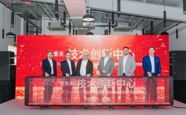
Balluff opens new technology center in Chengdu
With around 400 square meters of laboratory and office space, the center focuses on the development of sensor technologies, in particular inductive sensors and position measuring systems.
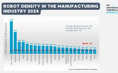
Global robot density: Western Europe leads ahead of North America and Asia
In the EU-27, the robot density is 231, which is above the global average of 132.