High-NA-EUV for global microchip production
The first machine for the new lithography technology includes an optical system from Zeiss and was recently delivered by ASML.
Together with its strategic partner ASML, the Dutch manufacturer of lithography systems, the Zeiss Semiconductor Manufacturing Technology (SMT) segment has now created the basic prerequisites for the production of integrated circuits at a new level. With the so-called High-NA-EUV lithography, significantly smaller structures can be realized on the carriers of the microchips – the wafers – and thus even more powerful, energy-efficient and cost-effective chips can be produced. The first series production using the new technology is set to begin in 2025.
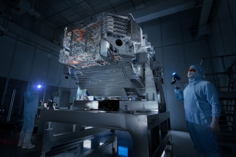
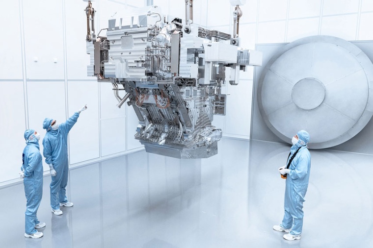
Zeiss has invested around ten million man-hours in research and development for High-NA-EUV lithography. Strategic partner ASML and many other European partners are also involved in the development of the technology. “We’re always working on pushing the boundaries of what's technically feasible,” states Andreas Pecher, member of the Zeiss executive board as president and CEO of the SMT segment. “Our aim is to actively shape digitalization worldwide with our innovations by enabling the chip industry to make new technological leaps. We’ve set ourselves ambitious goals to achieve this. Our perseverance over more than 25 years has now paid off: ASML’s new wafer scanner for the High-NA-EUV lithography is the most modern, complex and precise machine for microchip production in the world – and we’re very proud to provide the optical system as the heart of this machine.”
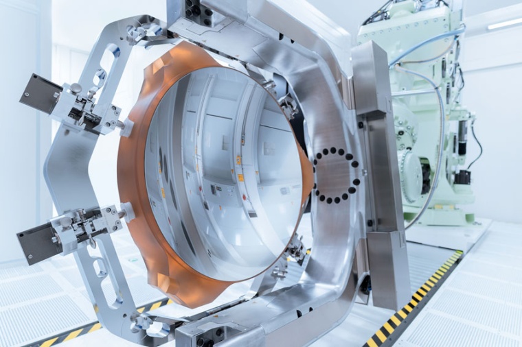
“Thanks to the larger numerical aperture and the new mirrors for the High-NA-EUV lithography, we can capture more light and thus expose it with even greater detail and precision. Experience has shown that the smaller the chip structures are to be, the larger the optical system consisting of projection optics and illumination system will be,” says Dr Peter Kürz, head of the High-NA-EUV lithography business at Zeiss SMT. The illumination system for that technology consists of around 25,000 parts and weighs more than six tons. With more than 40,000 parts, the projection optics weigh around twelve tons and ensure high-precision focusing of the light in the wafer scanner.
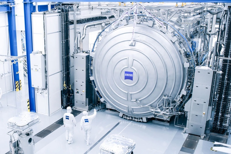
The most precise measurement technology in the world is needed to check the quality of the mirrors. “That kind of measurement technology didn’t exist, so we developed it together with ASML in parallel with the High-NA-EUV lithography. To this extent, we carried out some really pioneering work worldwide,” says Kürz. “This is the most complex machine we’ve ever produced at Zeiss.” In vacuum chambers with a diameter of around five meters, the measuring machine – weighing 150 tons in total – checks the quality of the mirrors with nanometer precision.
Company
Carl Zeiss SMT GmbHRudolf-Eber-Str. 2
73447 Oberkochen
Germany


most read

Heitec takes over Artschwager + Kohl
Through the acquisition, the company aims to expand its range of warehouse logistics solutions and open up new market segments.

Steute Technologies buys Kiepe Industry
Steute Technologies, backed by Battery Ventures, has acquired the industrial switching technology specialist and part of Kiepe Electric GmbH

Helukabel becomes Helu
Managing Director Marc Luksch emphasizes that the future of connection technology lies in the integration of ready-to-connect systems.
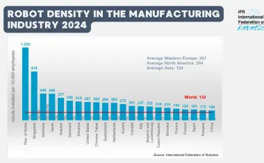
Global robot density: Western Europe leads ahead of North America and Asia
In the EU-27, the robot density is 231, which is above the global average of 132.

5 robotics trends for 2026
The International Federation of Robotics reports on the five most important trends for the robotics industry in 2026.