

IDS moves into new technology center
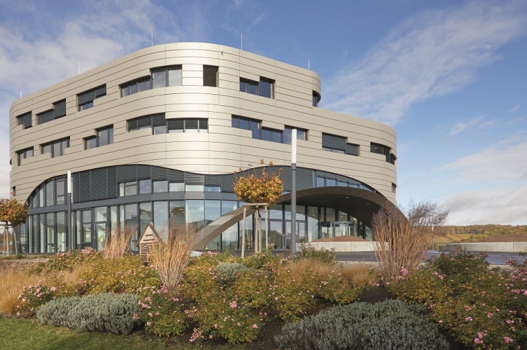
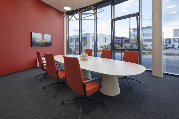
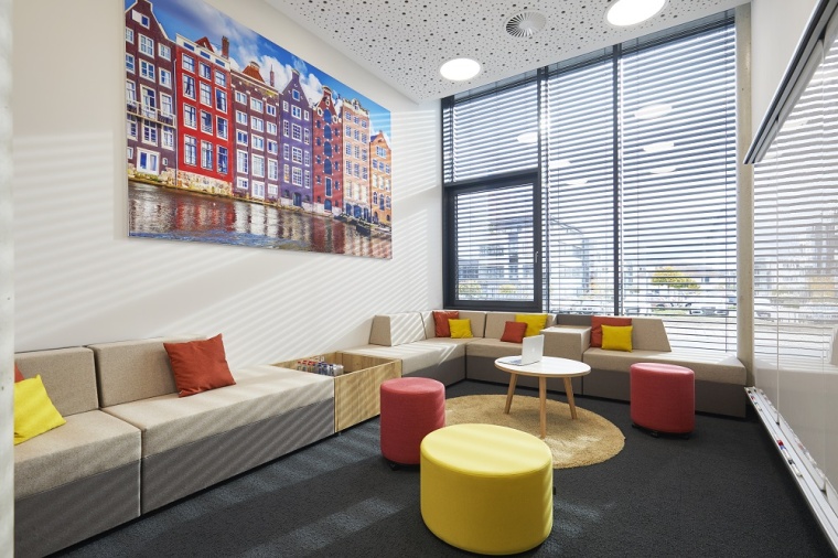
IDS has expanded its headquarters in Obersulm-Willsbach - after around one and a half years of construction, the technology center b39 was ready to move into. A total of 52 offices and six completely differently designed conference rooms as well as an event room with space for up to 200 people are located on a total area of more than 4500 square meters. The multi-storey car park behind the building is also new and has 262 parking spaces and charging stations for electric cars.
One aspect of the new building is its use as a platform for further training. The b39 Academy, a new branch of IDS, has its headquarters there. The aim is to jointly promote the development of digital specialist, method and technical skills, for example through event cooperation and knowledge transfer on topics such as image processing technology and artificial intelligence. Contacts to early-stage startups are also in focus.
Company
IDS Imaging Development Systems GmbHDimbacher Str. 10
74182 Obersulm
Germany

most read

European machine vision expects slight recovery and growth in 2026
According to the VDMA Machine Vision department, sales are expected to increase by around 3%, following a decline of 2% in 2025.
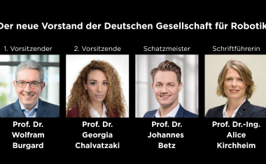
German Society for Robotics Elects First Regular Board of Directors Under Wolfram Burgard
The German Society for Robotics has elected its first regular board of directors. Starting in October, Wolfram Burgard will assume the presidency of the young professional society.

Solid-State Transformers for AI Data Centers
As part of a strategic partnership, Siemens and Reinhausen are developing a solid-state transformer for AI data centers with an 800-volt DC system.

Vision Components Celebrates 30 Years of Machine Vision with an Anniversary Event at Vision 2026
Vision Components is celebrating 30 years in business. At Vision 2026, the manufacturer is hosting an anniversary celebration featuring an exhibition, live music, and new products.
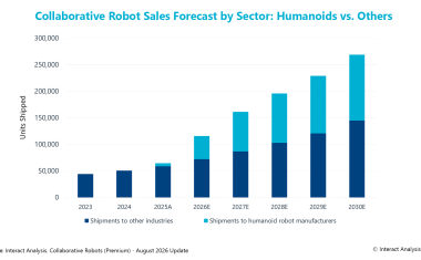
Humanoid robotics is driving demand for cobot arms and actuators
According to recent analyses, global production of humanoid robots exceeded the 20,000-unit mark in 2025 and is expected to more than triple in 2026.