New germanium-tin transistor as alternative to silicon
In experiments, the germanium-tin transistor exhibits a very high electron mobility.
Over the past seventy years, the number of transistors on a chip has doubled approximately every two years according to Moore’s Law, which is still valid today. The circuits have become correspondingly smaller, but an end to this development appears to be in sight. “We have now reached a stage where structures are only two to three nanometers in size. This is approximately equal to the diameter of ten atoms, which takes us to the limits of what is feasible. It doesn’t get much smaller than this,” says Qing-Tai Zhao of the Peter Grünberg Institute (PGI-9) at Forschungszentrum Jülich. For some time now, researchers have been looking for a substitute for silicon, the primary material used in the semiconductor industry. “The idea is to find a material that has more favourable electronic properties and can be used to achieve the same performance with larger structures,” he explains.
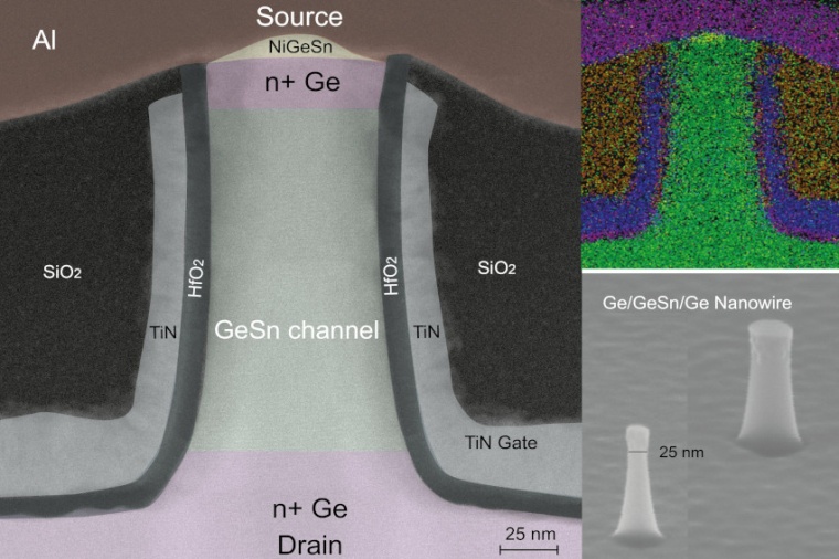
The research is in part focused on germanium, which was already being used in the early days of the computer era. Electrons can move much faster in germanium than in silicon, at least in theory. However, Qing-Tai Zhao and his colleagues have now gone one step further. To optimize the electronic properties even further, they incorporated tin atoms into the germanium crystal lattice. The method was developed several years ago at the Peter Grünberg Institute (PGI-9) of Forschungszentrum Jülich.
“The germanium-tin system we have been testing makes it possible to overcome the physical limitations of silicon technology,” says Qing-Tai Zhao. In experiments, the germanium-tin transistor exhibits an electron mobility that is 2.5 times higher than a comparable transistor made of pure germanium. Another advantage of the new material alloy is that it is compatible with the existing CMOS process for chip fabrication. Germanium and tin come from the same main group in the periodic table as silicon. The germanium-tin transistors could therefore be integrated directly into conventional silicon chips with existing production lines.
Apart from classical digital computers, quantum computers could also benefit from the germanium-tin transistor. For some time, there have been efforts to integrate parts of the control electronics directly on the quantum chip, which is operated inside a quantum computer at temperatures close to absolute zero. Measurements suggest that a transistor made of germanium-tin will perform significantly better under these conditions than those made of silicon. “The challenge is to find a semiconductor whose switching can still be very fast with low voltages at very low temperatures,” explains Qing-Tai Zhao. For silicon, this switching curve flattens out below 50 Kelvin. Then, the transistors need a high voltage and thus a high power, which ultimately leads to failures of the sensitive quantum bits because of the heating. “Germanium-tin performs better at these temperatures in measurements down to twelve Kelvin, and there are hopes to use the material at even lower temperatures,” says Qing-Tai Zhao.
In addition, the germanium-tin transistor is a further step towards optical on-chip data transmission.The transmission of information with light signals is already standard in many data networks because it is considerably faster and more energy-efficient than data transfer via electrical conductors. In the field of micro- and nanoelectronics, however, data is usually still sent electrically. Colleagues from the Jülich working group of Dan Buca have already developed a germanium-tin laser in the past that opens up the possibility to transmit data optically directly on a silicon chip. The germanium-tin transistor, along these lasers, provides a promising solution for the monolithic integration of nanoelectronics and photonics on a single chip. (Source: FZJ)
References: M. Liu et al.: Vertical GeSn nanowire MOSFETs for CMOS beyond silicon, Commun. Eng. 2, 7 (2023); DOI: 10.1038/s44172-023-00059-2 • A. Elbaz et al.: Ultra-low-threshold continuous-wave and pulsed lasing in tensile-strained GeSn alloys, Nat. Phot. 14, 375 (2020); DOI: 10.1038/s41566-020-0601-5