New lasers for digital holography
MultiLambdaChip project gets underway with Hübner Photonics, Carl Zeiss, Cybertechnologies, University of Freiburg, and the Fraunhofer IPM.
Modern optical measurement techniques such as digital holography enable inline quality assurance. Until now, the size and cost of the light sources have prevented these measurement techniques from becoming widely established. As part of the MultiLambdaChip research project, Fraunhofer Institute for Physical Measurement Techniques IPM in Freiburg, Germany, is developing highly integrated, cost-effective laser light sources for use in digital holography, working in collaboration with companies Hübner Photonics, Carl Zeiss, and Cybertechnologies, and the laboratory for optical systems at the University of Freiburg.
The quality assurance of critical components is becoming more and more challenging: An ever wider range of components has to be surveyed at ever shorter cycle rates with ever higher levels of precision – and, ideally, directly on the production line. Optical measurement techniques are best suited to this task. However, the size and cost of the required laser light sources are often limiting factors to using these techniques on a wider scale. In order to find a solution to this problem, Fraunhofer IPM has recently launched the MultiLambdaChip project together with four partners.
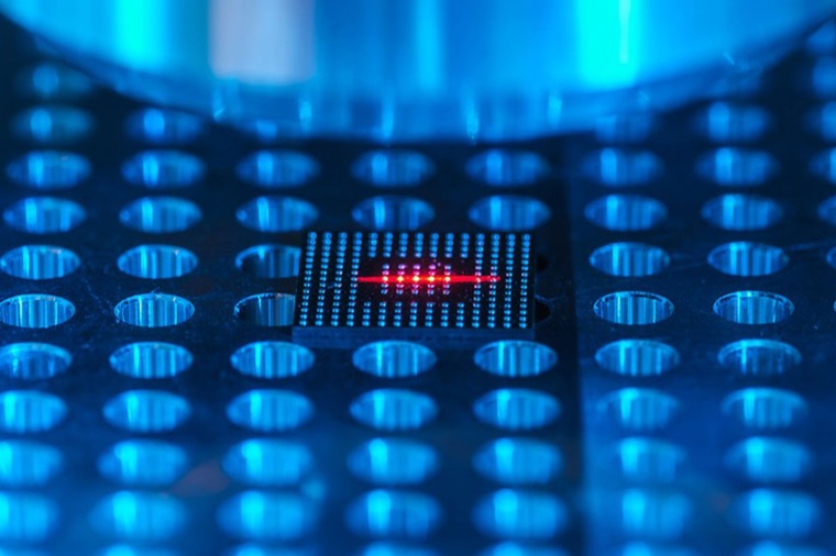
The project team aims to develop a new lithium niobate-based photonic circuit to produce a highly integrated, cost-effective and flexible multiwavelength laser light source. The plan is to manipulate and convert the 1,550 nm light of an inexpensive type of laser diode normally used in telecommunications and enable it to take high-precision measurements in the visible spectral range. This cost-effective light source will make the use of holographic measurement systems cost-efficient for many new tasks in modern production.
High-tech industries rely on many critical components with low tolerances being produced at high cycle rates. The production of microchips or high-performance electronics for e-mobility or renewable energy applications are good examples. Digital holography can, in principle, ensure reliable quality control in these scenarios. The light source being developed as part of MultiLambdaChip will make demanding in-line measuring tasks more and more affordable.
The project sets out to prove the operational capability of the new laser light source used in combination with holographic measurement systems for two specific industrial applications. Firstly, a novel holographic line sensor is designed to enable quality assurance during bake-out of microchips for the first time. Secondly, a holographic sensor system capable of taking comprehensive measurements is due to be integrated into a multiaxis handling system to allow the dimensional accuracy of ceramic components to be 100-percent controlled.
Achieving these objectives will, for the first time, make it possible to take high-precision in-line 3D measurements that could previously only be carried out in special measuring rooms.