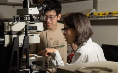
Better control in additive manufacturing
The elastic properties depend on structure size, process and fabrication parameters.
Additive manufacturing (AM) using two-photon polymerization lithography (TPP) has increased in usage in industry and research. Currently, a major constraint of TPP in general and specifically of the material IP-Q from Nanoscribe, Germany, is the users’ limited access to knowledge about material properties. Due to the nature of the process, the elastic properties in particular depend not only on the utilized material but also on structure size, process, and fabrication parameters. For example, no degree of conversion (DC) and Young’s modulus (E) values for IP-Q had been reported up to now.
A common approach uses a combination of Raman spectroscopy and nanoindentation to characterize the DC of monomer to polymer measurable via Raman spectroscopy, which can then be related to the mechanical behavior of the material, measurable via nanoindentation. Ongoing research on acoustic metagratings and metamaterials fabricated on MEMS would benefit from optimized elastic parameters to provide adjustability of the acoustic behavior, as they affect the characteristic acoustic impedance directly. AM encompasses processes with which objects can be created three-dimensionally from a technical drawing. The data are sent to an AM system, which then performs the fabrication.
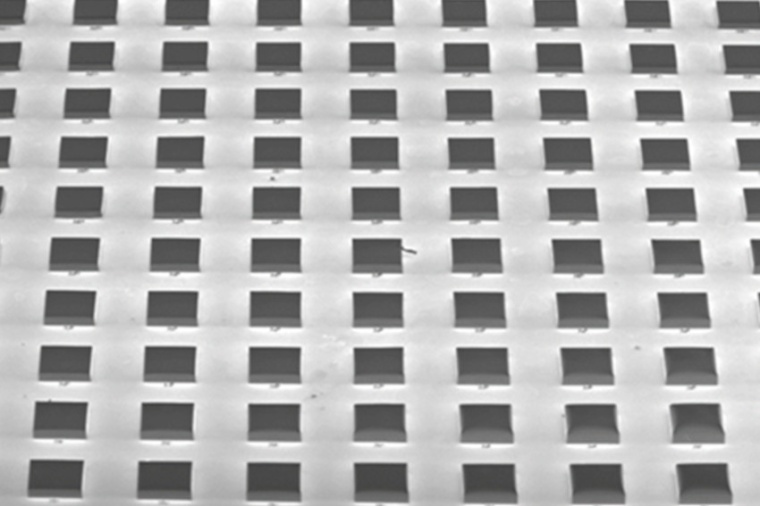
AM via TPP is based on selective curing of a liquid precursor to create solid structures inside a drop of monomer. Afterwards, the leftover liquid is washed away. Well known TPP applications are optical sub-micron structures, where the photoresist IP-Dip is commonly utilized. The more recently developed photoresist IP-Q was designed by the same manufacturer for larger applications, e.g. mounts, molds, and structural metamaterials. Sample structures from each of the two photoresists were produced in parameter sweeps. This allows the comparison of process parameters to the resulting characteristics. Raman spectroscopy was employed, which is a non-contact analysis method for material characterization in which monochromatic light is scattered off the material.
The reflection comprises not only the irradiated wavelength but also Raman scattering. The characteristic peaks of the Raman scattering spectrum can be used for the identification of chemical substances. In our work, it was used to determine the ratio of monomer to polymer – or DC – in the TPP samples. Micro- and nanoindentation were used to test the mechanical properties of the samples. A hard tip whose mechanical properties are known is pressed into the sample whose properties are unknown. From the slope of the load vs. displacement curve, E values were computed.
Finally, parameter sweeps of cuboid sample structures fabricated using TPP were investigated across the parameters laser power and scan speed to find dependent properties. The employed photoresists were examined using Raman spectroscopy to find the DC of monomer to polymer, and subsequently micro- or nanoindentation were used to find E. For IP-Dip, the attained DC and E ranged from 20 to 45 % and 1 to 2.1 Gigapascal, respectively. The results were compared to reports found in the literature. For IP-Q, the attained DC and E ranged from 53 to 80 % and 0.5 to 1.3 Gigapascal, respectively. The characterized properties of IP-Q manifest as the current state of knowledge of the material.
“By this means, offering an approach to optimize elastic parameters of TPP-fabricated structures will be beneficial for various ongoing research topics. A promising application for this method is the characterization of the elastic parameters of acoustic metagratings and metamaterials fabricated on MEMS. These devices can subsequently be implemented beneficially in life science, mobility, and industrial applications,” said Severin Schweiger of Fraunhofer Institute of Photonic Microsystems and Brandenburg University of Technology in Germany. (Source: SPIE)
Link: Fraunhofer-Institute for Photonic Microsystems IPMS, Dresden, Germany • Nanoscribe GmbH & Co. KG, Eggenstein-Leopoldshafen, Germany