Crystalline light catchers
New project to advance perovskite-based optoelectronics, such as solar cells, photodetectors, and LEDs.
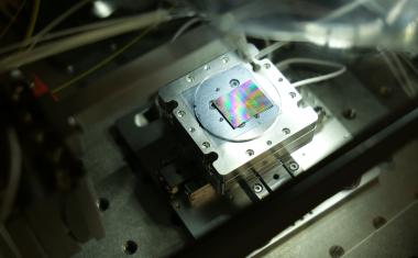
Various solutions are available for converting sunlight directly into electricity. The best known are silicon solar cells, which are based on silicon single crystals. Solar cells of this type are relatively thick and fragile. As a further variant, thin-film solar cells have emerged, which are about a hundred times thinner than crystalline silicon cells. This cell structure is flexible and can be vapor-deposited onto flexible substrates such as plastic films or metal foils. The thin-film cells made of the semiconductors gallium arsenide (GaAs), cadmium telluride (CdTe) or copper indium gallium sulfur selenium (CIGS) have now been joined by a new class: organic-inorganic perovskites. The term perovskite describes the common crystal structure of the materials in these thin films.
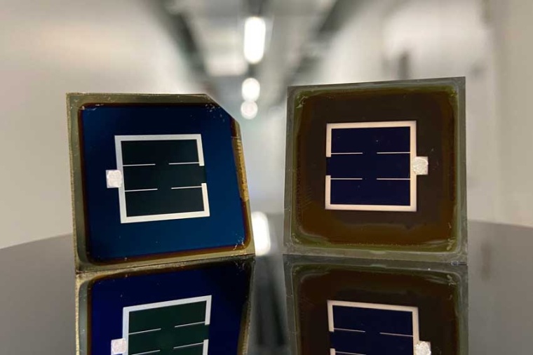
The interesting thing is that perovskites can not only be used as solar cells, but conversely can also serve as illuminators or as a basis for photodetectors, for example in X-ray devices or sensors for smartwatches. For this reason, this class of materials is currently attracting a lot of research activity worldwide. But there is a problem: Many of these perovskite crystals contain so-called organic ions as building blocks. These are crystal building blocks that contain carbon, nitrogen and hydrogen. They melt and evaporate at much lower temperatures than silicon or GaAs, CdTe or CIGS. As a result, many well-proven production methods are not well-suited for these materials.
The project Advanced Manufacturability of Hybrid Organic-inorganic Semiconductors for Large Area Optoelectronics AMYS which was launched as part of the Strategic Focus Area Advanced Manufacturing (SFA-AM) is now trying to solve precisely these problems. What is needed is an industrial manufacturing method for perovskite thin films, which have so far been produced mainly in “wet” processes in laboratories.
Industrial manufacturing
The tasks of the research partners are carefully distributed: Perovskite specialists Ayodhya Tiwari and Fan Fu’s team from Empa’s Thin Films and Photovoltaics Laboratory is looking for a flexible perovskite photodetector and solar cells; Chih-Jen Shih's team from ETH Zurich's Nanomaterials Engineering Research Group wants to build perovskite LEDs that produce light with particularly high color accuracy. And Christophe Ballif of EPFL and his team are on the hunt for particularly efficient tandem solar cells that consist of silicon on the bottom and a semi-transparent perovskite layer on top.
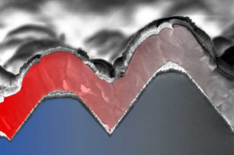
All the researchers have already done preliminary work: The EPFL team set a new world record in July: EPFL solar cells made of thick, crystalline silicon with a thin layer of perovskite on top achieved more than 31 percent efficiency. Such a value has already been achieved with other semiconductor cells, but these are about a thousand times more expensive to produce. So this opens a gateway to low-cost photovoltaics. “We have developed a two-step process to apply the organic ingredients of our perovskites gently and homogenously, on medium sized solar cells,” explains Christian Wolff, who works on the EPFL team. “We now want to extend this process to a newly developed dry vapor-based method, which will enable to homogeneously cover even larger areas on the one hand, and at the same time see if there are not even better chemical combinations.”
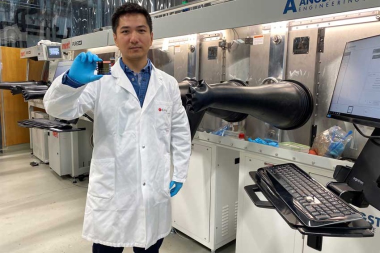
Sebastian Siol at Empa is helping him with this. He is a specialist in coating processes and in the analysis of industrially produced thin films. He will use automated high-throughput experiments to screen a large number of different chemical compositions and process parameters with the goal to create a “library” of promising perovskite mixtures. This will give Wolff and his colleagues in all working groups crucial tips on where to look. That speeds up the journey to the goal of cheap, stable and large-area optoelectronic devices with a manifold of applications.
Company
EmpaUeberlandstrasse 129
8600 Duebendorf
Switzerland

most read
Flexible Thermal Cameras for Use in Industry
Thermography is now essential in industrial workflows. With advanced cameras and intelligent algorithms, thermal imaging can be tailored to processes and opens new opportunities for manufacturers.
The Rise of Photonic and Neuromorphic Computing: A New Era for AI Hardware
Computer Architectures for future data processing
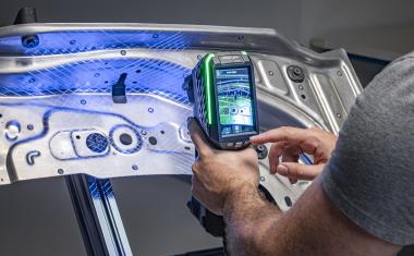
Portable Metrology for Quality Control
Creaform’s new Handyscan 3D|EVO Series offers portable, metrology‑grade 3D scanning for precise, efficient inspection. It helps QC/QA teams measure complex parts without CMM bottlenecks.
Automatic Defect Detection in Laser Welding and Brazing with AI
Process Monitoring in Automotive Production.
Systematic Characterization of Ring-Shaped Laser Beams
New metrics for meaningful analysis beyond ISO 11146.