Doubling down on metasurfaces
New bilayer device of titanium dioxide can control many forms of polarized light.
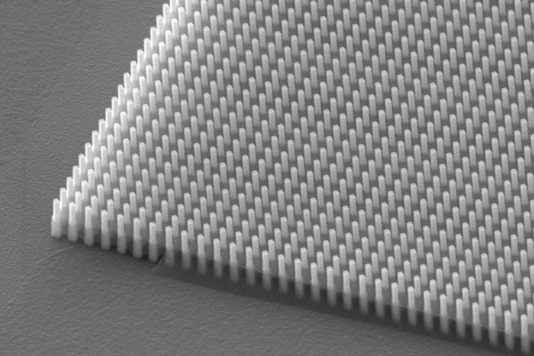
Almost a decade ago, Harvard engineers unveiled the world’s first visible-spectrum metasurfaces – ultrathin, flat devices patterned with nanoscale structures that could precisely control the behavior of light. A powerful alternative to traditional, bulky optical components, metasurfaces today enable compact, lightweight, multifunctional applications ranging from imaging systems and augmented reality to spectroscopy and communications. Now, researchers in the Harvard John A. Paulson School of Engineering and Applied Sciences (SEAS) are doubling down, literally, on metasurface technology by creating a bilayer metasurface, made of not one, but two stacked layers of titanium dioxide nanostructures. Under a microscope, the new device looks like a dense array of stepped skyscrapers.
“This is a feat of nanotechnology at the highest level,” said Federico Capasso. “It opens up a new way to structure light, in which we can engineer all its aspects such as wavelength, phase and polarization in an unprecedented manner…It signifies a new avenue for metasurfaces that so far has been just scratching the surface.” The SEAS-led metasurface development of the last decade has produced flat, ultrathin structures patterned with millions of tiny elements that can manipulate light with nanometer precision. A striking example technology is the metalens: Unlike conventional lenses, metalenses can be fabricated with existing semiconductor manufacturing, making possible compact, integrated optical systems in devices like smartphones, cameras, and augmented reality displays.
After Capasso’s team reported their first working metalens that can bend visible light, they worked with Harvard’s Office of Technology Development to license the technology and start a company, Metalenz. They’ve since demonstrated a host of potential applications, including an endoscope, an artificial eye, and a telescope lens. But the single-layer nanostructure design Capasso’s team invented has been in some ways limiting. For example, previous metasurfaces put specific requirements on the manipulation of light’s polarization in order to control the light’s behavior.
“Many people had investigated the theoretical possibility of a bilayer metasurface, but the real bottleneck was the fabrication,” said Alfonso Palmieri. With this breakthrough, Palmieri explained, one could imagine new kinds of multifunctional optical devices – for example, a system that projects one image from one side and a completely different image from the other. Using the facilities of the Center for Nanoscale Systems at Harvard, the team that included former postdoctoral researchers Ahmed Dorrah and Joon-Suh Park came up with a fabrication process for freestanding, sturdy structures of two metasurfaces that hold strongly together but do not affect each other chemically. While such multi-level patterning has been common in the silicon semiconductor world, it had not been as well explored in optics and metaoptics.
To demonstrate the power of their device, the team devised an experiment in which they used their bilayer metalens to act on polarized light in the same way that a complicated system of waveplates and mirrors does. In future experiments, the team could expand into even more layers to exert control over other aspects of light, such as extreme broadband operation with high efficiency across the entire visible and near infrared spectrum, opening the door to even more sophisticated light-based functionalities. (Source: Harvard SEAS)