European supply chain for diamond-based quantum technologies
The members of a joint research project are developing innovative processes and equipment to enable the industrial use of (111)-oriented diamond substrates.
To ensure the availability of high-purity as well as large-area diamond wafers for quantum technology applications, the project consortium of GrodiaQ (short for: Large-area diamond substrates for quantum technology) has started its work. The consortium is coordinated by the Fraunhofer Institute for Applied Solid-State Physics IAF and consists further of five companies with their own expertise in the field of manufacturing, processing and utilization of diamond and diamond-based quantum technologies. Together, the project partners cover the entire value chain. The aim is to develop manufacturing equipment and basic materials for quantum devices that can be commercially exploited by the industrial partners at the end of the project. The German Federal Ministry of Education and Research (BMBF) is funding the project for three years.
“Large-area high-quality diamond wafers are an irreplaceable basic component in the production of devices for diamond-based quantum technologies, which are expected to reach the market in the next three to ten years,” explains the responsible project coordinator from Fraunhofer IAF, Dr Peter Knittel. “Material costs can be significantly reduced by using diamond wafers with larger diameters compared to the current state of the art, making the development and production of quantum devices economical. Against this background, GrodiaQ is a great opportunity to establish Germany as a leading location in the research, development and production of advanced diamond-based quantum technologies.”
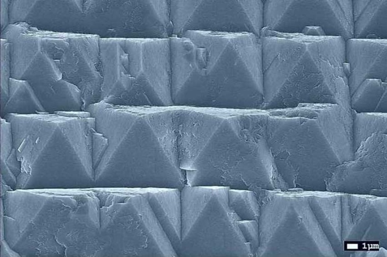
Specific material properties enable nitrogen-vacancy centers (NV centers) in diamond to form stable quantum states already at room temperature. For this reason, the use of NV centers in diamond substrates is one of the most promising approaches on the way to the application and economic exploitation of quantum technologies, for example in areas such as medical technology (quantum sensing) or computer science (quantum computing). In particular, diamond grown in the (111)-oriented crystal direction is an important material for the fabrication of quantum devices, as this growth both favors the generation of NV centers by facilitating nitrogen incorporation and significantly improves their controllability as qubits.
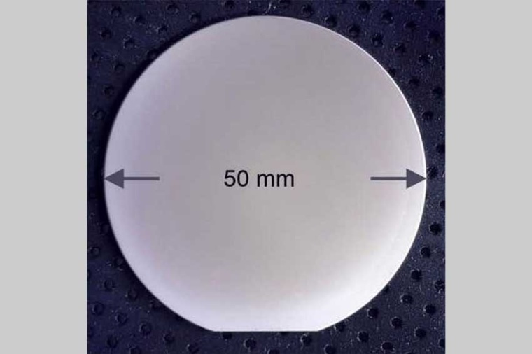
However, the supply of diamond substrate that fulfills the above-mentioned conditions is still problematic. Only a few manufacturers – none of them from the European Union (EU) – can supply material at all that meets the described requirements for crystal purity and (111) orientation. Availability is also limited to non-industrial small quantities and dimensions of typically 3x3 mm. The fragility of the available substrates is also a hurdle as they must be polished to a surface roughness of less than 2 nm for applications in quantum technologies. In contrast, the diamond wafers planned in GrodiaQ are characterized by an industrially suitable size that are at the same time, as a result of optimized processing procedures, ideal substrates for further preparation and processing.
European supply chain for sovereign material supply
In three steps, the GrodiaQ project partners want to enable industrially usable diamond substrates and thereby lay the foundation for a European supply chain for quantum devices. In addition to the project coordination, Fraunhofer IAF provides material, know-how and infrastructure throughout the entire project duration. Furthermore, it focuses on optimizing the heteroepitaxial growth of (111)-oriented diamond in order to be able to produce functional layers for quantum technology applications. In close cooperation with Fraunhofer IAF, Diamond Materials is responsible for grinding and polishing down to a roughness of less than 2 nm as well as growth and processing of larger substrate areas and quantities.
Evatec Europe is designing and constructing an energy-efficient reactor for chemical vapor deposition (CVD) based on the bias-enhanced nucleation (BEN) approach, which, in combination with new semiconductor microwave generators from Trumpf Hüttinger, is intended to achieve industrial standards for wafer coating from sizes of four inches. The quality of the diamond coatings depends to a large extent on the chamber geometry and voltage distribution of the BEN reactor, and the homogeneity of the microwave plasma over a larger area depends on the generators. Finally, the associated partners Q.ant and Quantum Brilliance will evaluate the substrates characterized at the IAF with regard to their applications in the fields of quantum sensing and quantum computing and will transfer them to the market after the project.
Company
Fraunhofer Institute for Applied Solid State Physics IAFTullastraße 72
79108 Freiburg
Germany


most read
inspect America July 2025 is now available!
In this issue, we provide a comprehensive review of Automate, highlighting the most cutting-edge trends, products, and market insights.

B&R products now available in Europe through RS
B&R has entered into a strategic partnership with RS to distribute B&R products through RS's online and offline channels.
Europe's automotive industry is increasingly focusing on automation
The European automotive industry continues to invest heavily in the automation of its production, as preliminary figures from the International Federation of Robotics (IFR) show.
Quantum technologies on the rise
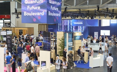
World of Quantum 2025 in Munich recorded impressive growth with 160 exhibitors from 16 countries and over 22,000 visitors from 41 countries.
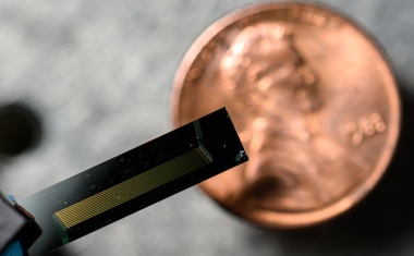
Tiny laser measures objects at ultrafast rates
The chip-scale laser has applications ranging from guiding autonomous vehicles to detecting gravitational waves.