Gentle crystallization of sensitive silicon layers
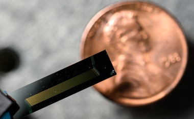
A new process eliminates the need for wires and solder joints, an advantage that can significantly reduce the component size and enhance the sensor performance.
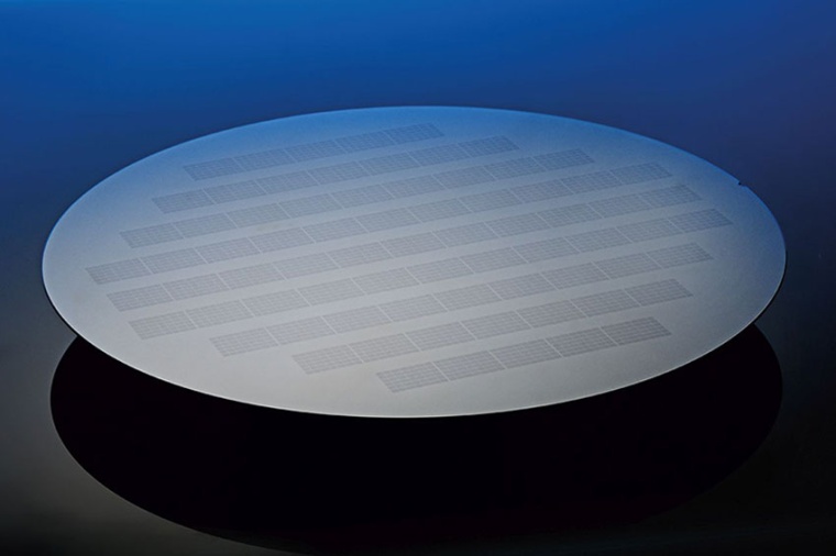
We owe safe and reliable car journeys to MEMS sensors since they record many key parameters of vehicle operation. They make it possible to control many vehicle systems such as airbags, anti-lock brakes or electronic stability programs. To measure acceleration, etc., MEMS inertial sensors are also incorporated into consumer products such as smartphones, smartwatches, quadrocopters, etc. by the billions. So that MEMS sensor units can perform these tasks reliably and safely, they are combined with an electronic, application-specific integrated circuit (ASIC) that sits on a silicon carrier unit (wafer).
To make these MEMS even more powerful in the future, researchers at the Fraunhofer Institute for Laser Technology ILT in Aachen have developed a CMOS-compatible deposition and laser crystallization process in collaboration with the Fraunhofer ISIT and IST.
However, because the ambient temperature near the integrated circuit with its temperature-sensitive CMOS transistors may not exceed 450 °C, MEMS sensors made of crystalline silicon are first manufactured separately due to the conventionally high manufacturing temperatures. Then they are contacted with the circuit via wire and solder connections or wafer bonding processes. “But conventional interconnection technology requires a relatively large amount of space and prevents further miniaturization of the MEMS,” explains Florian Fuchs, a research associate in the thin film processing group at Fraunhofer ILT. For this reason, MEMS made of crystalline silicon cannot be built directly on the ASIC. The temperature incompatibilities in the manufacturing process make it difficult to further miniaturize the sensors and enhance their performance.
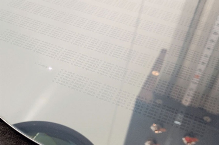
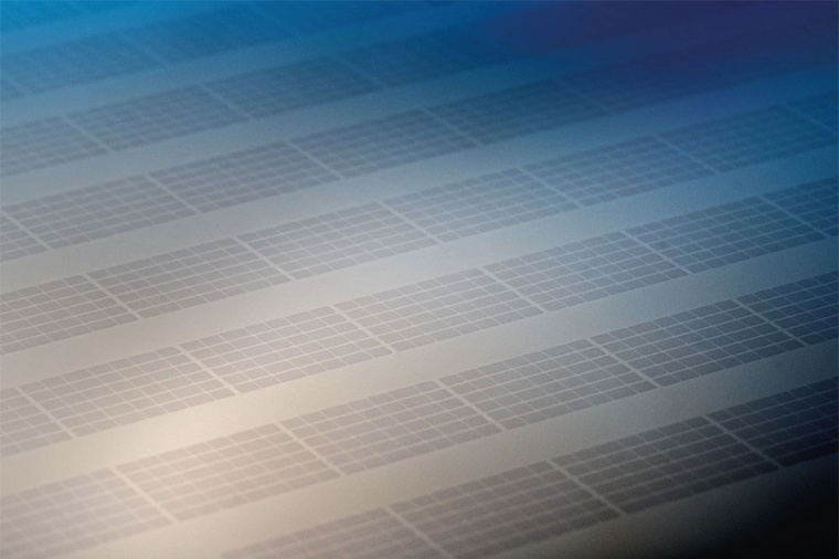
Instead of using conventional joining techniques, Fraunhofer ILT is relying on a laser-based process which enables it to build MEMS sensors of crystalline silicon directly (monolithically) on the temperature-sensitive circuits. The project focuses on the deposition of Si layers by Fraunhofer IST and ISIT, selective laser crystallization by Fraunhofer ILT, and the design and microelectronic processing of the layers into sensors by Fraunhofer ISIT. The researchers are taking advantage of the fact that amorphous silicon layers can already be produced on the wafer holding the circuit at temperatures below 450 °C and high deposition rates. The laser not only crystallizes this silicon layer, but also activates the dopants it contains, thus ensuring suitable electrical conductivity. Subsequently, the sensor units are processed further using classic microelectronic manufacturing processes.
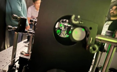
When laser radiation is used to crystallize silicon at high-temperature, but below its melting point, crystallization occurs spatially, selectively and very quickly (in the lower millisecond range). This way – in conjunction with targeted temperature management – the process minimizes mechanical stresses in the layer material, but does not damage the sensitive electronics on the underlying substrate. The silicon is crystallized with a focused laser beam that has a diameter of a few 10 µm and guided by a mirror to scan the entire surface step by step. In this spatially selective process, heat is removed effectively in three spatial directions. This distinguishes the process from alternative photonic processes such as flash exposure (flash lamp), where heat can only be dissipated in one direction because the area to be processed is so large.
“Since the energy is quickly introduced into only a small volume, we achieve solid phase crystallization of the silicon with laser processing at temperatures that are actually above the destruction threshold of the underlying circuit. Due to the short local processing time, the circuit is nevertheless not damaged,” explains Dr Christian Vedder, head of the thin film processing group at Fraunhofer ILT. The newly developed laser process reduces the electrical resistances of the silicon layers by more than four orders of magnitude, down to below a value of 0.05 Ω·cm. At a layer thickness of 10 µm, this value corresponds to a sheet resistance of 50 Ω/sq. MEMS sensors with typical finger structures for a capacitive acceleration sensor could be produced from these layers.
This opens interesting applications for the automotive industry, medical technology and fire departments.
Company
Fraunhofer Institute for Laser Technology ILTSteinbachstr. 15
52074 Aachen
Germany


most read
Optical knots made of laser beams
Interference patterns between overlapping laser beams could transmit encoded information over thousands of feet through chaotic environments.

Europe's automotive industry is increasingly focusing on automation
The European automotive industry continues to invest heavily in the automation of its production, as preliminary figures from the International Federation of Robotics (IFR) show.
Tiny laser measures objects at ultrafast rates
The chip-scale laser has applications ranging from guiding autonomous vehicles to detecting gravitational waves.
Quantum technologies on the rise
World of Quantum 2025 in Munich recorded impressive growth with 160 exhibitors from 16 countries and over 22,000 visitors from 41 countries.

B&R products now available in Europe through RS
B&R has entered into a strategic partnership with RS to distribute B&R products through RS's online and offline channels.