High-throughput, low-cost surface production
Project LAMpAS presents the first laser system that can achieve controlled topographic characteristics.
The EU-funded LAMpAS project has successfully developed the first laser system, based on Interference Patterning combined with a polygon scanner system, for high-throughput, low-cost surface production with controlled topographic characteristics. This new concept of laser machine can produce well-defined surface patterns with controlled length scales and feature sizes in order to provide surfaces with advanced functions.
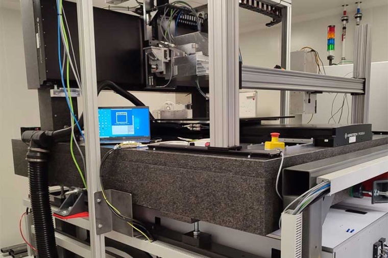
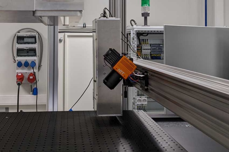
The new laser machine consists of several important modules, including:
High-power ps-laser source: a 1.5 kW laser system has been developed by Trumpf, with 1 – 3 ps pulse durations and a reduced spectral bandwidth required for direct laser interference patterning (DLIP). The laser source can provide pulse energies up to 4 mJ, making it ideal for this application.
Advanced laser surface texturing optics: for the first time worldwide, a unique optical head was constructed, which combines of a polygon scanner specially designed by Scanlab with a direct laser interference patterning unit from TU Dresden. The module allows the fabrication of periodic textures at high throughput, producing hierarchical patterns for surface functionalization.
Real-time surface characterization module: two real-time monitoring systems were developed which are based from one side on a near-infrared camera as well as a camera system which can monitor the structuring process in real time. Furthermore, they can detect heat-accumulation or indirectly predict in real time the depth of produced topographies with a resolution of about 15 nm.
LAMpAS was set up in 2019 with a grant of 5.1 million euros under the EU’s Horizon 2020 program. The aim of this project was to develop new concepts for laser structuring and to bring the technology to industrial levels at affordable costs. It aimed at the design of newly functionalized surfaces by enhancing the efficiency, flexibility and productivity of processes based on the development of a high power ultrashort-pulsed laser system together with advanced optical concepts for high-throughput materials processing.
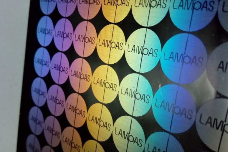
Inspired by nature, LAMpAS technology aimed to produce well-defined periodic surface patterns with feature sizes smaller than 1 µm that can provide tailored surface functions for applications including antifingerprint, decorative and easy to clean finishes for ovens, fridges and other home appliances.
Company
European Photonics Industry Consortium EPIC17 Rue Hamelin
75016 Paris
France


most read
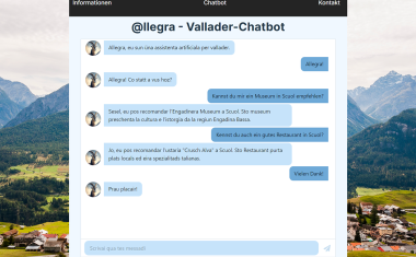
Chatbots for Dead, Endangered, and Extinct Languages
Possibilities and Limitations of Generative AI for Continuing Education.
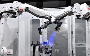
3D laser scanning for 100 percent inspection
Modern production requires precise, fast, and fully automated inspection processes. The robot-assisted inline measurement system Flexscan meets this requirement with two 3D compact sensors

It Does Not Always Have to Be a Humanoid Robot
Mythomorphic design adds a distinct perspective to social robotics. Inspired by myths and fantasy rather than humans or animals, the article classifies examples and examines related opportunities and risks.
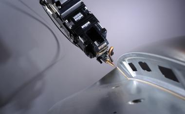
Automatic Defect Detection in Laser Welding and Brazing with AI
Process Monitoring in Automotive Production.

Protective Windows: Finding a Germanium Alternative for LWIR Imaging
In this interview, Mike Giznik, President of Midopt, explains why Silwir is a good choice for applications such as industrial inspection, defense, and autonomous systems.