The quantum twisting microscope
New tool can visualize the quantum electronic waves of two twisted atomically-thin layers directly.
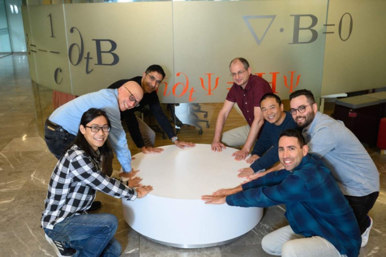
Researchers from the Weizmann Institute of Science make use of the wave–particle duality to develop a new type of tool – the quantum twisting microscope (QTM) – that can create novel quantum materials while simultaneously gazing into the most fundamental quantum nature of their electrons. The study’s findings may be used to create electronic materials with unprecedented functionalities. The QTM involves the twisting or rotating of two atomically-thin layers of material with respect to one another.
In recent years, such twisting has become a major source of discoveries. It began with the discovery that placing two layers of graphene, one atop the other with a slight relative twist angle, leads to a sandwich with unexpected new properties. The twist angle turned out to be the most critical parameter for controlling the behavior of electrons: Changing it by merely one-tenth of a degree could transform the material from an exotic superconductor into an unconventional insulator. But critical as it is, this parameter is also the hardest to control in experiments. By and large, twisting two layers to a new angle requires building a new sandwich from scratch, a process that is very long and tedious.
“Our original motivation was to solve this problem by building a machine that could continuously twist any two materials with respect to one another, readily producing an infinite range of novel materials,” says Shahal Ilani of Weizmann’s condensed matter physics department. “However, while building this machine, we discovered that it can also be turned into a very powerful microscope, capable of seeing quantum electronic waves in ways that were unimaginable before.”
“Many different scanning probes have been developed, each measuring a different electronic property, but all of them measure these properties at one location at a time. So, they mostly see electrons as particles, and can only indirectly learn about their wave nature,” explains Ady Stern, who took part in the study along with three other theoretical physicists from the same department: Binghai Yan, Yuval Oreg and Erez Berg. “As it turned out, the tool that we have built can visualize the quantum electronic waves directly, giving us a way to unravel the quantum dances they perform inside the material,” Stern says.
“The trick for seeing quantum waves is to spot the same electron in different locations at the same time,” says Alon Inbar. “The measurement is conceptually similar to the famous two-slit experiment, which was used a century ago to prove for the first time that electrons in quantum mechanics have a wave nature,” adds John Birkbeck. “The only difference is that we perform such an experiment at the tip of our scanning microscope.”
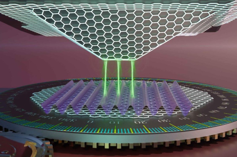
To achieve this, the researchers replaced the atomically sharp tip of the scanning tunneling microscope with a tip that contains a flat layer of a quantum material, such as a single layer of graphene. When this layer is brought into contact with the surface of the sample of interest, it forms a two-dimensional interface across which electrons can tunnel at many different locations. Quantum mechanically, they tunnel in all locations simultaneously, and the tunneling events at different locations interfere with each other. This interference allows an electron to tunnel only if its wave functions on both sides of the interface match exactly. “To see a quantum electron, we have to be gentle,” says Ilani. “If we don’t ask it the rude question ‘Where are you?’ but instead provide it with multiple routes to cross into our detector without us knowing where it actually crossed, we allow it to preserve its fragile wave-like nature.”
Generally, the electronic waves in the tip and the sample propagate in different directions and therefore do not match. The QTM uses its twisting capability to find the angle at which matching occurs: By continuously twisting the tip with respect to the sample, the tool causes their corresponding wave functions to also twist with respect to one another. Once these wave functions match on both sides of the interface, tunneling can occur. The twisting therefore allows the QTM to map how the electronic wave function depends on momentum, similarly to the way lateral translations of the tip enable the mapping of its dependence on position. Merely knowing at which angles electrons cross the interface supplies the researchers with a great deal of information about the probed material. In this manner they can learn about the collective organization of electrons within the sample, their speed, energy distribution, patterns of interference and even the interactions of different waves with one another.
“Our microscope will give scientists a new kind of lens for observing and measuring the properties of quantum materials,” says Jiewen Xiao. The Weizmann team has already applied their microscope to studying the properties of several key quantum materials at room temperature and is now gearing up toward doing new experiments at temperatures of a few kelvins, where some of the most exciting quantum mechanical effects are known to take place. Peering so deeply into the quantum world can help reveal fundamental truths about nature. In the future, it might also have a tremendous effect on emerging technologies. The QTM will provide researchers with access to an unprecedented spectrum of new quantum interfaces, as well as new eyes for discovering quantum phenomena within them. (Source: Weizmann Inst.)
Reference: A. Inbar et al.: The quantum twisting microscope, Nature 614, 682 (2023); DOI: 10.1038/s41586-022-05685-y
Link: Dept. of Condensed Matter Physics, Weizmann Institute of Science, Rehovot, Israel


most read
Microvista expands management team with new dual leadership
Dr. Robin Höhne joins company founder Prof. Dr. Lutz Hagner as Chief Executive Officer.
Change in management at Stemmer Imaging: Arne Dehn steps down
New interim CEO Paul Scholten takes over management

Qioptiq Photonics becomes Excelitas Germany
The renaming is part of the global consolidation of the Excelitas Group.

HMS Networks takes over Industrial Communications division from Molex
This strategic acquisition includes intellectual property in hardware and software, a product portfolio with network cards and software stacks, as well as customer relationships in the USA and Japan.

Electrical and digital industry calls for strategy for Europe's digital sovereignty
The French and German electrical and digital industry associations, FIEEC and ZVEI, are calling for a proactive strategy for Europe's digital sovereignty.