Zeiss Microscopy opens Semiconductor Applications Lab
State-of-the-art innovation laboratory in Dresden, Germany, pushes the limits of advanced semiconductor applications.
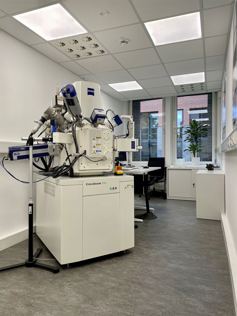
Zeiss has recently opened its Microscopy semiconductor applications lab in Dresden, a state-of-the-art facility dedicated to addressing physical analysis challenges and pushing the limits of nanoscale analysis with the Crossbeam focused ion beam-scanning electron microscope (FIB-SEM).
The new facility is strategically located in Dresden, the heart of semiconductor innovation within Europe, allowing for close collaboration with semiconductor industry customers and partners on physical failure analysis, materials development and process yield improvement for advanced logic and memory, power semiconductors, MEMS, advanced packaging, and more. The company will address increased automation of microscopy workflows and advanced techniques to help the semiconductor industry accelerate root cause analysis and pathfinding for the most challenging issues in microelectronics.
This laboratory in Dresden is the third major investment of Zeiss into semiconductor microscopy applications and strengthens the company’s global support capabilities. The Dresden team collaborates closely with its counterparts in Taiwan and Korea to share knowledge and best practices to best address customer needs across these three global hotspots of semiconductor excellence. Importantly, the advanced applications developed by these three teams will steer the innovation roadmap to meet the greatest challenges facing lab professionals in the semiconductor industry.
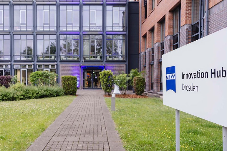
The semiconductor microscopy applications lab is located within the Innovation Hub Dresden that opened last May. The site complements Zeiss’ Innovation Center in Hsinchu Science Park, Taiwan, which opened in June 2024 and features a comprehensive portfolio to meet the productivity needs of semiconductor research and development, production and failure analysis. The third Innovation Center is in Dongtan, Korea, where the company develops applications across a complete portfolio of optical and electronic equipment, X-ray microscopy and high-resolution CT, and 3D metrology instruments.
Further reading: Zeiss expands its Innovation Hub in Dresden, wileyindustrynews.com, 17 May 2024 • Werner von Siemens Ring goes to Zeiss and Trumpf, wileyindustrynews.com, 18 September 2024
Company
Carl Zeiss AGCarl-Zeiss-Str. 22
73447 Oberkochen
Germany


most read
Europe's automotive industry is increasingly focusing on automation
The European automotive industry continues to invest heavily in the automation of its production, as preliminary figures from the International Federation of Robotics (IFR) show.
Tiny laser measures objects at ultrafast rates
The chip-scale laser has applications ranging from guiding autonomous vehicles to detecting gravitational waves.
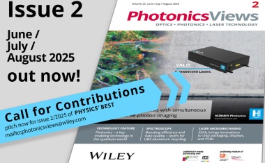
PhotonicsViews issue 2/2025 is out!
Pitch or submit your story for the fall issue of PHYSICS' BEST – out 20 October 2025

Successful trade fair for photonics and innovation
Laser World of Photonics 2025 in Munich ended with record figures and an optimistic outlook for the industry.
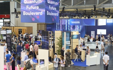
Quantum technologies on the rise
World of Quantum 2025 in Munich recorded impressive growth with 160 exhibitors from 16 countries and over 22,000 visitors from 41 countries.