3D laser nanoprinters become compact
Two-step absorption replaces two-photon absorption as the primary optical excitation process
Lasers in conventional laser printers for paper printouts are very small. 3D laser printers for 3-dimensional microstructures and nanostructures, by contrast, have required big and expensive laser systems so far. Researchers of Karlsruhe Institute of Technology (KIT) and the Heidelberg University now use another process for this purpose. Two-step absorption works with inexpensive and small, blue laser diodes. As a result, much smaller printers can be used.
-
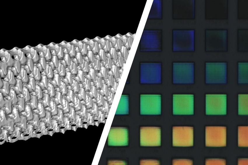 Electron microscopic reconstruction of a 3D nanostructure printed with the 2-step absorption process (l.) and the nanostructures under a light microscope. (Source: R. Schröder, U. Heidelberg / V. Hahn, KIT)
Presently, laser printing is the method of choice for additive manufacture by 3D printing, as it offers the best spatial resolution of all methods and reaches an extremely high printing speed. In laser printing, a focused laser beam is directed towards a light-sensitive liquid. At the focal point, the laser light turns a switch in special molecules and triggers a chemical reaction. The reaction leads to the local hardening of the material. By moving the focal point, any 3D micro- and nanostructures can be produced. The chemical reaction is based on two-photon absorption, meaning that two photons excite the molecule at the same time, which causes the desired chemical modification. However, this simultaneous excitation happens very rarely, which is why complex pulsed laser systems have to be applied, resulting in bigger dimensions of the laser printer.
When using the two-step process, more compact, smaller printers can be realized. The first photon transfers the molecule to an intermediate state. In the second step, a second photon transfers the molecule from the intermediate state to the desired excited state and starts chemical reaction. The advantage: Contrary to two-photon absorption, the absorption of the two photons must not necessarily happen at the same time. “For the process, compact and low-power continuous-wave laser diodes can be used,” says Vincent Hahn. The required laser powers are far below those of conventional laser pointers. Printing, however, requires specific photoresists. “Development of these photoresists has taken several years and has been possible only in collaboration with chemists,” says KIT-researcher Martin Wegener.
To Martin Wegener, the advantage is obvious: “It is a big difference between using a femtosecond laser as large as a big suitcase for several ten thousand euros or a semiconductor laser that is as large as a pinhead and costs less than ten euros. Now, the other components of the 3D laser nanoprinter also have to be miniaturized. To me, a device that will be as large as a shoebox appears realistic in the next years. That would be even smaller than the laser printer on my desktop at KIT.” This way, 3D laser nanoprinters might become affordable for many groups. Experts are already talking about a democratization of 3D laser printing technology. (Source: KIT)