Business unit moves from Fraunhofer FEP to Fraunhofer IPMS
12.03.2024 - The microdisplays and sensors branch transfers to the neighboring sister institute to bundle competencies, leverage synergies.
By pooling expertise and streamlining structures, the two Fraunhofer institutes anticipate the creation of synergies that will strengthen the research field, expedite development and thus benefit customers and partners. Both institutes are closely connected, particularly within this business unit, and share infrastructure at the Dresden site.
-
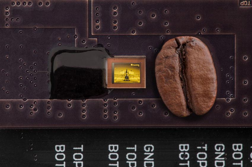 OLED microdisplay with a resolution of 1440 × 1080 pixels and the world’s smallest pixels of 2.5 micrometers (Source: C. Jacquemin / Fh. IPMS)
 -
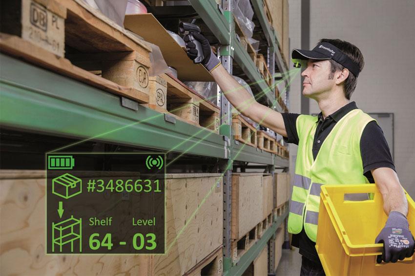 Microdisplays for logistics applications (Source: C. Jacquemin / Fh. IPMS)
There is rapid development in the market for the microdisplays used in augmented reality (AR), virtual reality (VR) and mixed reality (MR) applications – often collectively referred to as extended reality (XR) – and this will be an important growth market of the future. The integration of OLED and µLED frontplane technologies in CMOS backplanes is not only the key to success in this sector but also the technological basis for near-to-eye visualization of information. IPMS and FEP have now decided, in consultation with the Fraunhofer-Gesellschaft, to integrate the Microdisplays and Sensors business unit into Fraunhofer IPMS. Their goal is to leverage synergies in the area of infrastructure, pool expertise and establish a unique profile for both institutes. IPMS has long been one of the leading institutes in microelectronics and microsystems engineering.
Over the past ten years, the Microdisplays and Sensors business unit has developed into a globally successful and established player under the umbrella of Fraunhofer FEP. At the current stage of development, the transfer to an institute specialized in microelectronics offers suitable conditions to further develop the business unit. This will also allow Fraunhofer FEP, as a process-oriented institute, to focus even more on its expertise in electron beam and plasma technology. This transfer provides technological solutions for the growing demand in the fields of energy, sustainability, life sciences and environmental technologies for industry and society — now and in the future.
“By integrating the Fraunhofer FEP Microdisplays and Sensors business unit into Fraunhofer IPMS, we are pooling our expertise and ensuring the best possible use of our infrastructure. This will also increase our chances to win projects with the Microelectronics group. The transfer is a good example of the strategic development of a research field and the leveraging of synergies across institutes,” says Prof Holger Hanselka, president of the Fraunhofer-Gesellschaft. “This will strengthen the research field and pave the way for new technological capabilities in the field of microdisplays by leveraging the synergies of the existing microelectronics infrastructure. The close relationship of the institutes at the Dresden site will ensure seamless and continuous advancement in this field. My special thanks go to all those involved for their contributions.”
Harald Schenk, director of Fraunhofer IPMS, added: “In the future, Fraunhofer IPMS will increase its activities in this area and focus more on the heterogeneous integration of various chiplet technologies in conjunction with CMOS microelectronics. This future-oriented technology includes the integration of organic semiconductors (e.g., OLEDs) and novel emitter technologies (e.g., µLEDs), which will open up new avenues in micro/optoelectronics and microsystems engineering.”
Elizabeth von Hauff, director of Fraunhofer FEP, said: “The Microdisplays and Sensors business unit has played a significant role in Fraunhofer FEP’s dynamic development. We are proud of this and would like to thank our employees and managers for their dedication. Transferring to the IPMS will open up additional development potential for the business unit and enable Fraunhofer FEP to focus on strategic topics in the field of electron beam and plasma technologies.”
Contact
Fraunhofer Institut für Photonische Mikrosysteme IPMS
Maria-Reiche-Str. 2
01109 Dresden
Germany
+49 351 8823-0
+49 351 8823-266
Fraunhofer-Institut für Organische Elektronik, Elektronenstrahl- und Plasmatechnik FEP
Winterbergstraße 28
01277 Dresden
Germany
+49 351 2586-0
+49 351 2586-105