New process to stack micro-LEDs
Approach ist based on 2D materials to create LED displays with smaller and thinner pixels.
Put on a virtual reality headset and, chances are, it will look like you are viewing the world through a screen door. Current flat panel displays use pixels that are visible to the naked eye, along with small bits of unlit dark space between each pixel that can appear as a black, mesh-like grid. Now, researchers from the Georgia Institute of Technology, in collaboration with researchers from the Massachusetts Institute of Technology (MIT), have developed a new process based on 2D materials to create LED displays with smaller and thinner pixels. Enabled by two-dimensional, materials-based layer transfer technology, the innovation promises a future of clearer and more realistic LED displays.
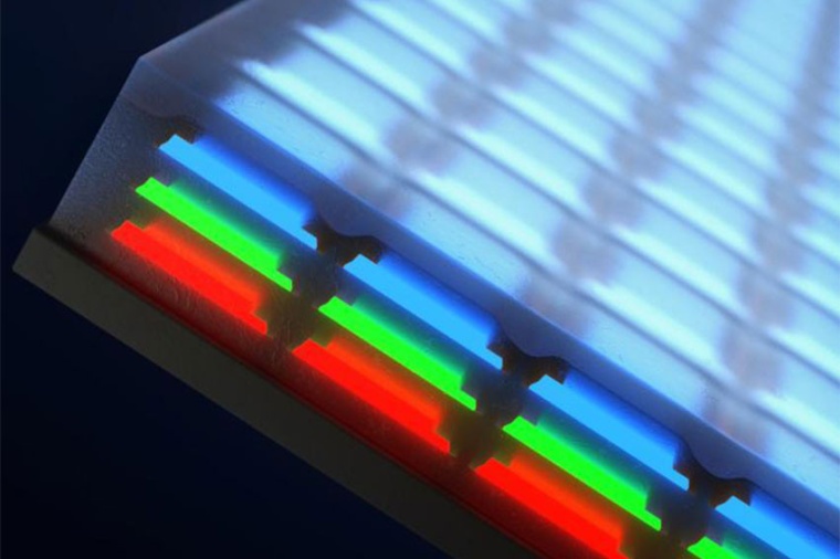
Abdallah Ougazzaden and Suresh Sundaram from Georgia Tech collaborated with researchers from MIT to turn the conventional LED manufacturing process on its head – literally. Instead of using prevailing processes based on laying red, green, and blue (RGB) LEDs side by side, which limits pixel density, the team vertically stacked freestanding, ultrathin RGB LED membranes, achieving an array density of 5,100 pixels per inch – the smallest pixel size reported to date (4 microns) and the smallest-ever stack height – all while delivering a full commercial range of colors. This ultra-small vertical stack was achieved via the technology of van der Waals epitaxy on 2D boron nitride developed at the Georgia Tech-Europe lab and the technology of remote epitaxy on graphene developed at MIT.
They showed that the world’s thinnest and smallest pixeled displays can be enabled by an active layer separation technology using 2D materials such as graphene and boron to enable high array density micro-LEDs resulting in full-color realization of micro-LED displays. One unique facet of the two-dimensional, material-based layer transfer (2DLT) technique is that it allows the reuse of epitaxial wafers. Reusing this costly substrate could significantly lower the cost for manufacturing smaller, thinner, and more realistic displays.
“We have now demonstrated that this advanced 2D, materials-based growth and transfer technology can surpass conventional growth and transfer technology in specific domains, such as in virtual and augmented reality displays,” said Ougazzaden. These advanced techniques were developed in metalorganic chemical vapor deposition (MOCVD) reactors, the key tool for LED production at the wafer scale. The 2DLT technique can be replicated on an industrial scale with high throughput yield. The technology has the potential to bring the field of virtual and augmented reality to the next level, enabling the next generation of immersive, realistic micro-LED displays.
“This emerging technology has a tremendous potential for flexible electronics and the heterogenous integration in optoelectronics, which we believe will develop new functionalities and attract industry to develop commercial products from smartphone screens to medical devices,” Ougazzaden said. (Source: Georgia Tech)