Super flexible semiconductors for printed displays
18.08.2023 - New composite semiconductor is made up of a water-insoluble polymer and indium oxide.
Scientists at the department of materials engineering, Indian Institute of Science (IISc), have developed a super flexible, composite semiconductor material that can have possible applications in next-generation flexible or curved displays, foldable phones and wearable electronics.
-
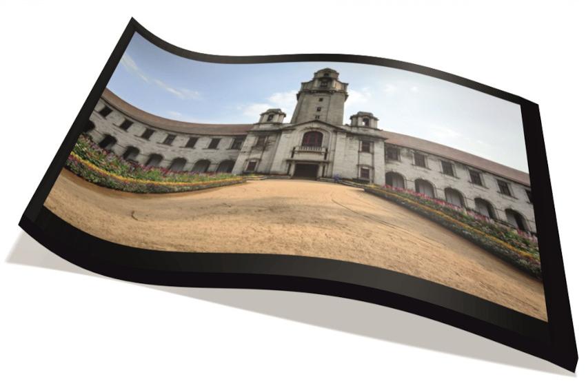 The composite semiconductor-based transistors on flexible Kapton substrate and envisioned fully printed flexible display. (Source: J. R. Pradhan)
 -
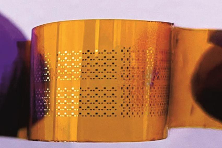 Detailed view of the composite semiconductor-based transistors on a flexible polymer substrate. (Source: J. R. Pradhan)
Traditional semiconductor devices used in display industries are either made of amorphous silicon or amorphous oxides, both of which are not flexible and strain tolerant at all. Adding polymers to the oxide semiconductors may increase their flexibility, but there is a limit to how much can be added without compromising the semiconductor’s performance. Now, the researchers have found a way to fabricate a composite containing a significant amount of polymer – up to 40 % of the material weight – using a solution-process technique, specifically inkjet printing. In contrast, previous studies have reported only up to 1-2 % polymer addition. Interestingly, the approach enabled the semiconducting properties of the oxide semiconductor to remain unaltered with the polymer addition. The added large quantity of polymer also made the composite semiconductor highly flexible and foldable without deteriorating its performance.
The composite semiconductor is made up of two materials – a water-insoluble polymer such as ethyl cellulose that provides flexibility, and indium oxide, a semiconductor which brings in excellent electronic transport properties. To design the material, the researchers mixed the polymer with the oxide precursor in such a way that interconnected oxide nanoparticle channels are formed around phase-separated polymer islands through which electrons can move from one end of a transistor to the other, ensuring a steady current flow. The key to form these connected pathways, the researchers found, was the choice of the right kind of water-insoluble polymer that does not mix with the oxide lattice when the oxide semiconductor is being fabricated.
“This phase separation and the formation of polymer-rich islands helps in crack arrest, making it super flexible,” says Subho Dasgupta. Semiconductor materials are usually fabricated using deposition techniques such as sputtering. Instead, Dasgupta’s team uses inkjet printing to deposit their material onto various flexible substrates ranging from plastics to paper. In the present study, the polymer material Kapton has been used. Just like words and images printed on paper, electronic components can be printed on any surface using special functional inks containing either electrically conducting, semiconducting or insulating materials.
However, there are challenges. “Sometimes it is very difficult to get a continuous and homogeneous film. Therefore, we had to optimise certain protocols, for example, preheating the printed semiconductor layer on the Kapton substrate prior to high temperature annealing,” explains Mitta Divya, a former PhD student. Another challenge is ensuring the right environmental conditions under which the ink can be printed. “If the humidity is too low, you can’t print, because the ink dries up within the nozzle,” says Subho Dasgupta.
He adds that in the future, such printed semiconductors can be used to fabricate fully printed and flexible television screens, wearables, and large electronic billboards alongside printed organic light emitting diode display front-ends. These printed semiconductors will be low-cost and easy to manufacture, which could potentially revolutionize the display industry. His team has obtained a patent for their material and plans to test its shelf-life and quality control from device to device before it can be scaled up for mass production. They also plan to look for other polymers that can help design such flexible semiconductors. (Source: IISC)
Link: Dept. of Materials Engineering, Indian Institute of Science (IISc), Bangalore, India