On-chip factory for single photons
New quantum method to generate single photons with higher efficiency at room temperature.
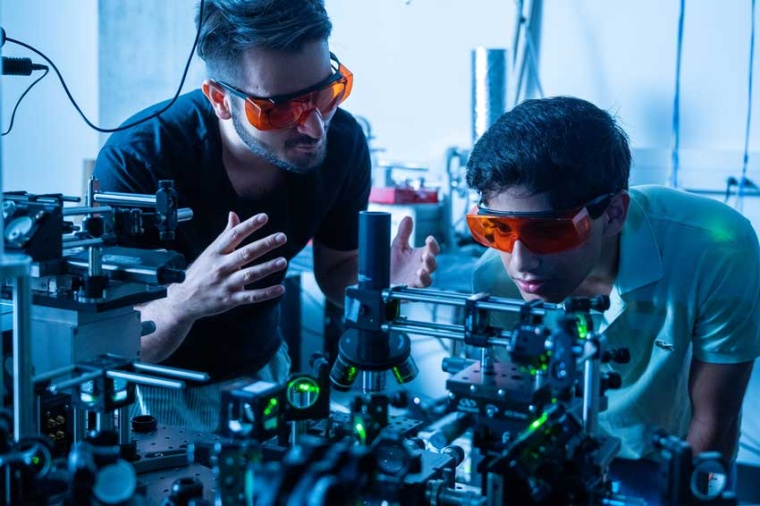
Quantum devices today are “about where the computer was in the 1950s,” which it is to say, the very beginning. That’s according to Kamyar Parto, Ph.D. student in the UC Santa Barbara lab of Galan Moody, an expert in quantum photonics. Parto describing a key advance: the development of a kind of on-chip “factory” for producing a steady, fast stream of single photons, essential to enabling photonic-based quantum technologies.
“In quantum technology you have superconducting qubits, spin qubits in silicon, electrostatic spin qubits and ion-trap-based quantum computers. Microsoft is trying to do topologically protected qubits, and in the Moody Lab, we’re working on quantum photonics”, Parto said. He predicts that the winning platform will be a combination of different platforms, given that each is powerful but also has limitations. “For instance, it’s very easy to transfer information using quantum photonics, because light likes to move,” he said. “A spin qubit, however, makes it easier to store information and do some local stuff on it, but you can’t move that data around. So, why don’t we try to use photonics to transfer the data from the platform that stores it better, and then transform it again to another format once it’s there?”
For qubits, the challenge is to generate and collect single photons with very high efficiency, such as by routing them on a chip using waveguides. Parto explained: “If we put these single photons into many different waveguides – a thousand single photons on each waveguide – and we sort of choreograph how the photons travel along the waveguides on the chip, we can do a quantum computation.” While it is relatively simple to use waveguides to route photons on chip, isolating a single photon is not easy, and setting up a system that produces billions of them rapidly and efficiently is much harder. The new technique employs a peculiar phenomenon to generate single photons with an efficiency that is much greater than has been achieved previously.
“The work is about amplifying the generation of these single photons so that they become useful to actual applications,” Parto said. “The breakthrough is that we can now generate the single photons reliably at room temperature in a way that lends itself to (the mass-production process of) CMOS.” There are various ways to go about generating single photons, but Parto and his colleagues are doing it by using defects in certain two-dimensional semiconductor materials. “If you shine light onto the right kind of defect, the material will respond by emitting single photons,” Parto said, adding, “The defect in the material acts as a rate-limiting state, which allows it to behave like a factory for pushing out single photons, one at a time.”
One photon might be produced as often as every three to five nanoseconds, but the researchers aren’t yet sure of the rate, and Parto says that the current rate could be much slower. A big advantage of 2D materials is that they lend themselves to having defects engineered into them at specific locations. Further, Parto said, “The materials are so thin that you can pick them up and put them on any other material without being constrained by the lattice geometry of a 3D crystal material. That makes the 2D material very easy to integrate.”
To make a useful device, the defect on the 2D material must be placed in the waveguides with extreme precision. “There is one point on the material that produces light from a defect,” Parto noted, “and we need to get that single photon into a waveguide.” Researchers try to do that in a couple of ways, for instance, by putting the material on the waveguide and then looking for an existing single defect, but even if the defect is precisely aligned and in exactly the right position, the extraction efficiency will be only 20 % to 30 %. That is because the single defect can emit only at one specific rate, and some of the light is emitted at oblique angles, rather than directly along the path to the waveguide. The theoretical upper limit of that design is only 40 %, but making a useful device for quantum-information applications requires 99.99 % extraction efficiency.
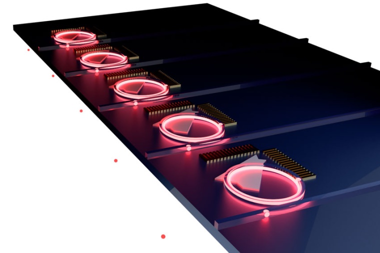
“The light from a defect inherently shines everywhere, but we prefer that it shine into these waveguides,” Parto explained. “We have two choices. If you put waveguides on top of the defect, maybe ten to fifteen percent of the light would go into the waveguides. That’s not enough. But there is a physics phenomenon, the Purcell effect, that we can utilize to boost this efficiency and direct more of the light into the waveguide. You do that by placing the defect inside an optical cavity – in our case it’s in the shape of a micro-ring resonator, which is one of the only cavities that allows you to couple light into and out of a waveguide.
“If the cavity is small enough,” he added, “it will squeeze out the vacuum fluctuations of the electromagnetic field, and those fluctuations are what cause the spontaneous emission of photons from the defect into a mode of light. By squeezing that quantum fluctuation into a cavity of finite volume, the fluctuation over the defect is increased, causing it to emit light preferentially into the ring, where it accelerates and becomes brighter, thus increasing the extraction efficiency.”
In experiments using the micro-ring resonator, the team achieved extraction efficiency of 46 %, which is an order-of-magnitude increase over prior reports. “We’re really encouraged by these results, because single-photon emitters in 2D materials address some of the outstanding challenges facing other materials in terms of scalability and manufacturability,” said Moody. “In the near term, we’ll explore using them for a few different applications in quantum communications, but in the long term, our goal is to continue to develop this platform for quantum computing and networking.”
To do that, the group needs to improve their efficiency to better than 99 %, and achieving that will require higher-quality nitride resonator rings. “To enhance efficiency, you need to smooth out the ring when you carve it out of the silicon nitride film,” Parto explained. “However, if the material itself is not fully crystalline, even if you try to smooth it at the atomic level, the surfaces could still look rough and sponge-like, causing the light to scatter off of them.”
While some groups achieve the highest-quality nitride by purchasing it from companies that grow it perfectly, Parto explained, “We have to grow it ourselves, because we have to put the defect under the material, and also, we’re using a special type of silicon nitride that minimizes the background light for single-photon applications, and the companies don’t do that.”
Parto can grow his nitrides in a plasma-enhanced chemical vapor deposition oven, but because it is a heavily used shared facility, he is not able to customize some settings that would allow him to grow material of sufficient quality. The, plan, he says, is to use these results to apply for new grants that would make it possible “to get our own tools and hire students to do this work.” (Source: UCSB)


most read

5 robotics trends for 2026
The International Federation of Robotics reports on the five most important trends for the robotics industry in 2026.

Agile Robots forms Krause Automation
Agile Robots has taken over the European and North American assets of Thyssenkrupp Automation Engineering and will continue to operate the business under the name Krause Automation.

Steute Technologies buys Kiepe Industry
Steute Technologies, backed by Battery Ventures, has acquired the industrial switching technology specialist and part of Kiepe Electric GmbH
Sick increases sales in 2025
In the 2025 financial year, the company increased its turnover to 1.85 billion euros, an increase of 6.5% compared to the previous year.
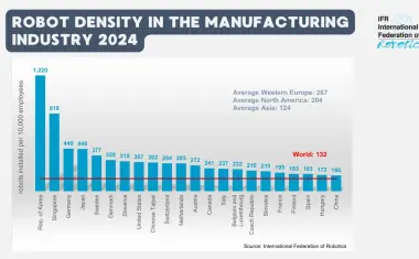
Global robot density: Western Europe leads ahead of North America and Asia
In the EU-27, the robot density is 231, which is above the global average of 132.