Environmentally friendly quantum dots for fast photodetectors
A novel method for synthesizing InSb/InP colloidal quantum dots stable under ambient conditions.
Applications such as lidar, 3D imaging for mobile devices, automotive and augmented/virtual reality or night vision for surveillance, rely on the development of short-wave infrared (SWIR) photodetectors. These devices are capable of operating in the spectral window of one to two microns. The SWIR light sensor industry has been dominated for years by the epitaxial technology, mainly based on devices made of indium gallium arsenide (InGaAs). However, several factors such as high production costs, low-scale manufacturability and incompatibility with CMOS has confined the epitaxial technology to niche and military markets. In contrast, the potential of SWIR photodetectors made of colloidal quantum dots (CQDs), nanoscale semiconductor materials, has attracted significant interest in the recent years due to their appealing features, such as low cost and compatibility with CMOS architecture, among others.
While this recent CQDs is emerging as a competitor technology for InGaAs based devices, it is important to clarify that current CQDs based SWIR photodetectors use components such as lead (Pb) and mercury (Hg) chalcogenides. Both of these elements are subject to the Restriction of Hazardous Substances (RoHS) European directive, which regulates their usage in commercial consumer applications. As a consequence of this regulatory framework, there is a pressing urge for the development of SWIR light sensors based on environmentally friendly, heavy-metal-free CQDs. Indium antimonide (InSb) CQDs have a great potential to deliver high- performance and stability devices. Moreover they are RoHS compliant and have access across the full SWIR range thanks to the low bandgap of bulk InSb. However, its synthesis has proven to be challenging so far due to the most strongly covalent nature of InSb and lack of the highly reactive precursors. Moreover, previous studies have reported that InSb CQDs are unstable upon exposure to air due to the strong propensity of Sb to oxidize.
Now, researchers from ICFO Lucheng Peng, Yongjie Wang, Yurong Ren, Zhuoran Wang, led by Gerasimos Konstantatos in collaboration with Pengfei Cao from Ernst Ruska Center for Microscopy and Spectroscopy with Electrons, describe a new method to synthesize arsenic free InSb CQDs with access to the SWIR range. Their approach includes the design of an InSb/InP core-shell structure of the synthesized quantum dots that are used to fabricate a fast-response and highly-sensitive SWIR photodetector. The researchers have developed a new synthetic process to produce high-quality wide spectral tunable InSb quantum dots with size uniformity by using commercially available chemical precursors, overcoming some of the hurdles that previous strategies had suffered, including a challenging synthesis process and high surface defect density.
The researchers adopted the single-source approach, using a continuous precursor injection process, instead of a hot injection option. This strategy was key to obtain InSb CQD with a well-controlled size distribution and distinct absorption over a very broad range of the spectrum. By using a range of reaction temperatures spanning from 220 ºC to 250 ºC, they were able to control the positions of the dots within the resulting solution-processed thin film. “The resultant spectral tuneability from near infrared to short-wave infrared, that is from 900 to 1750 nanometers, is the largest reported to date for InSb CQD”, the researchers explained. They observed the processed CQD samples with transmission electron microscopy (TEM) technique and confirmed that the dots had an average size of 2.4, 3.0, 3.5, 5.8 and 7.0 nanometers that enabled the absorption of different wavelengths. The researchers also characterized the surface of the InSb CQDs, since it is known to be crucial to the CQD material's optoelectronic properties. They used X-Ray photoelectron spectroscopy to investigate the oxidation states of Sb that are associated to the surface's unpassivated Sb dangling bonds and they could confirm the formation of Sb-oxide over the unprotected surface.
The next step in their investigation was to develop a passivation strategy to cover the obtained InSb CQDs creating a shell to protect the QCDs from oxidation. The surface of InSb QCDs was treated with indium trichloride (InCl3). This protected the surface dangling bonds of Sb by reducing the defects and improving at the same time the colloidal stability of the CQDs in the following steps of the purification process. Subsequently, the researchers grew indium phosphide (InP) protection shell with thin thickness over the purified InSb CQD. They used indium oleate and phosphine silylamide as precursors to generate the shell. This caused a significant red shift on the absorption spectrum of the InSb CQDs. The InSb/InP core-shell structure was confirmed later by the photoluminescence spectra analysis. “InSb/InP core-shell structure means growing another material (in this case, InP) on the surface of the pristine material (in this case, InSb). In comparison to InSb, InP is a wider bandgap material that can sufficiently passivate the surface traps of InSb that are detrimental in optoelectronic devices. Also, the Sb element is quite sensitive to oxygen, so the core-shell structure can largely improve the air stability of the material”, explains Lucheng Peng.
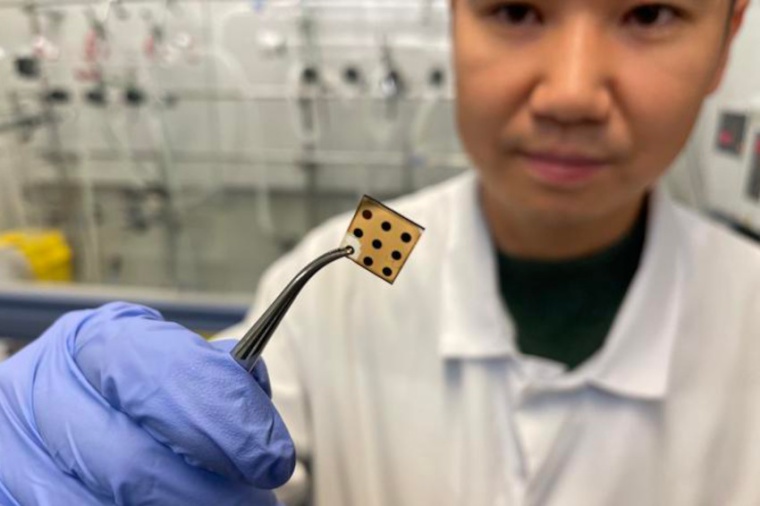
Once this first step was achieved, the researchers move onto using the optimized InSb/InP core-shell CQDs to fabricate a low temperature, high-speed SWIR photodetector. The light sensor device was formed by several stacked layers: a base of Indium Tin Oxide (ITO), an electron transfer layer (ETL) made by titanium dioxide (TiO2), the thin layer containing the InSb/InP CQDs and a final top layer made of gold. They wanted to obtain a photodetector with a fast time response to be used in applications that goes beyond video frame rates, so they used TiO2 as an ETL because its photochemical stability. The response of the fabricated light sensor was then measured. The photodetector demonstrates remarkable features including a wide linear dynamic range exceeding 128 dB, a maximum external quantum efficiency (EQE) of 25 % at 1240 nanometers and 12 % at 1420 nanometers, fast photoresponse time of 70 nanoseconds, and a specific detectivity of up to 4.4 × 10¹¹ Jones.”
As the researchers could verify, the device turned out to be highly resistant to atmospheric conditions without any encapsulation. After two months of exposure to the ambient environment, the photodetector maintained its properties. After 90 hours, the device's stability was also verified when it was functioning in the open air, and it was found to be extremely stable. “This is the best solution-processed, CQD SWIR photodetector based on InSb so far considering both performance and stability, with figures of merit that can enable high-frame-rate light sensors for machine vision, gated imaging and 3D sensing applications”, said Gerasimos Konstantatos. “The present study not only shows the enormous potential of InSb CQDs as an active material free of heavy metals to be used in SWIR photodetectors, but it also opens the door for future developments in colloidal InSb utilizing wet chemical methods towards the fabrication of high-performing electronic or optoelectronic devices”, he concluded.
The team is now working on how to further reduce the dark current and increase the quantum efficiency of the CQDs based photosensors. In order to do so, they mainly need to focus on improving the carrier mobility in the thin films that contain the CQDs. Achieving this will allow them to get a faster response speed for the light sensor, aiming to go beyond the 10 ns response speed so that the technology can be used in i-ToF (indirect-time-of-flight), which is useful in lidar and 3D imaging. (Source: ICFO)
Reference: L. Peng et al.: InSb/InP Core–Shell Colloidal Quantum Dots for Sensitive and Fast Short-Wave Infrared Photodetectors, ACS Nano, online 2 February 2024; DOI.10.1021/acsnano.3c12007
Further reading: Non-toxic quantum dots for infrared image sensors, WileyIndustryNews.com, 29. January 2024