Hexagonal boron nitride for quantum sensors
hBN has the potential to replace diamond as the preferential material for quantum sensing.
Diamond has long been the go-to material for quantum sensing due to its coherent nitrogen-vacancy centres, controllable spin, sensitivity to magnetic fields, and ability to be used at room temperature. With such a suitable material so easy to fabricate and scale, there’s been little interest in exploring diamond alternatives. But diamond is not an ideal material when exploring quantum sensors and information processing. When diamonds get too small, the super-stable defect it’s renowned for begins to crumble. There is a limit at which diamond becomes useless. Hexagonal boron nitride (hBN) has previously been overlooked as a quantum sensor and a platform for quantum information processing. This changed recently when a number of new defects were discovered that are shaping up to be compelling competitors to diamond’s nitrogen vacancy centers.
Of these the boron vacancy center – a single missing atom in the hBN crystal lattice – has emerged as the most promising to date. It can, however, exist in various charge states and only the -1 charge state is suitable for spin-based applications. The other charge states have, so far, been challenging to detect and study. This was problematic as the charge state can flicker, switching between the –1 and 0 states, making it unstable especially in the types of environments that are typical for quantum devices and sensors. But researchers from TMOS, the ARC Centre of Excellence for Transformative Meta-Optical Systems have developed a method to stabilize the –1 state, and a new experimental approach for studying the charge states of defects in hBN using optical excitation and concurrent electron beam irradiation.
Angus Gale says, “This research shows that hBN has the potential to replace diamond as the preferential material for quantum sensing and quantum information processing because we can stabilize the atomic defects that underpin these applications resulting in 2D hBN layers that could be integrated into devices where diamond can’t be.” Dominic Scognamiglio says, “We’ve characterized this material and discovered unique and very cool properties, but the study of hBN is in its early days. There are no other publications on charge state switching, manipulation or stability of boron vacancies, which is why we’re taking the first step in filling this literature gap and understanding this material better.”
Milos Toth says, “The next phase of this research will focus on pump-probe measurements that will allow us to optimize defects in hBN for applications in sensing and integrated quantum photonics.” Quantum sensing is a rapidly advancing field. Quantum sensors promise of better sensitivity and spatial resolution than conventional sensors. Of its many applications, one of the most criticial for Industry 4.0 and the further miniaturization of devices is precise sensing of temperature as well as electric and magnetic fields in microelectronic devices. Being able to sense sense these is key to controlling them. Thermal management is currently one of the factors limiting furthering the performance of miniaturised devices. Precise quantum sensing at the nanoscale will help prevent overheating of microchips and improve performance and reliability.
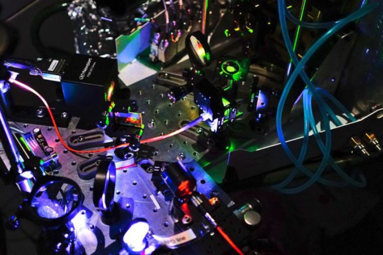
Quantum sensing also has significant applications in the medtech sphere, where its ability to detect magnetic nanoparticles and molecules could one day be used as an injectable diagnostic tool that searches for cancer cells, or it could monitor the metabolic processes in cells to track the impact of medical treatments. In order to study the boron vacancy defects in hBN, the team created a new experimental setup that integrated a confocal photoluminescent microscope with a scanning electron microscope (SEM). This allowed them to simultaneously manipulate the charge states of boron vacancy defects with the electron beam and electronic micro-circuits, whilst measuring the defect.
Gale says, “The approach is novel in that it allows us to focus the laser onto and image individual defects in hBN, whilst they are manipulated using electronic circuits and using an electron beam. This modification to the microscope is unique; it was incredibly useful and streamlined our workflow significantly.” (Source: TMOS)