Hyperspectral Imaging for Surface and Layer Analysis
16.06.2025 - Optical Wafer Inspection
-
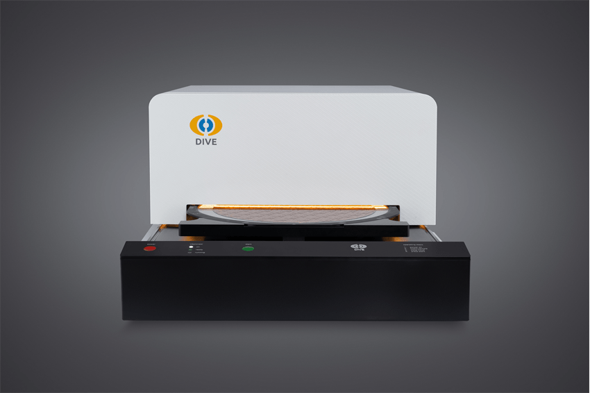 Dive’s Vepioneer Hyperspectral Vision System for non-destructive wafer inspection. Image: Dive Imaging Systems
 -
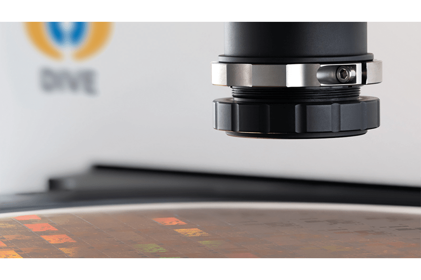 Specim FX hyperspectral camera in wafer inspection. Image: Dive Imaging Systems
By combining spectral analysis with high-resolution imaging, hyperspectral imaging enables full-surface, 100 percent inspection of wafers. This comprehensive approach detects layer thickness variations, contamination, and defects with exceptional accuracy. Hyperspectral imaging brings advanced, non-invasive inspection capabilities to the semiconductor industry and beyond. Direct inspection of production wafers leads to fewer defects, greater resource efficiency, and significantly faster inspection times.
In semiconductor manufacturing, hyperspectral imaging evaluates the spatial distribution of thin film thickness of oxides, resists, or surface parameters before or after every processing step in lithography or CVD/PVD/ALD processes. Combining detailed spectral data with high-resolution imaging enables a thorough analysis of wafer properties, ensuring quality and consistency.
Dive Imaging Systems is a German-based manufacturer of tools for surface and layer inspection in semiconductor production. It builds Hyperspectral Vision systems – integrating hardware, software, and comprehensive solutions for industrial inspection tasks. With a primary focus on performance surfaces and thin film applications, the company addresses the need for meticulous inspection and quality control in thin-layer application processes.
Any deviation from specifications can lead to malfunctions, making accurate assessment crucial. Dive’s technology offers a comprehensive evaluation of surface characteristics, particularly beneficial in semiconductor manufacturing. Beyond semiconductors, Dive’s technology caters to a wide range of industries, including electronics production, glass or foil coating for optics, encapsulation, and cleanliness of bonding surfaces.
Dr. Philipp Wollmann, CEO of Dive Imaging Systems, states, “Our goal is to offer a fully integrated hyperspectral imaging solution for industrial inspection, providing comprehensive insights on surface characteristics and layer parameters like thickness, with the aid of artificial intelligence and machine learning.”
With Dive’s solutions, the success of processing steps in semiconductor manufacturing can be tested directly on production wafers, significantly reducing the need for standard test wafers. Hyperspectral cameras are crucial in this integration.
Improved Quality, and Faster Inspection with Hyperspectral Imaging
Hyperspectral imaging had a profound impact on Dive’s system. By integrating Specim’s FX10 VNIR and FX17 NIR hyperspectral cameras, Dive has achieved high accuracy and speed in their wafer inspection processes. According to Wollmann, hyperspectral imaging provides several advantages in wafer inspection over traditional imaging methods: “Hyperspectral imaging offers a significant leap forward in wafer inspection by enabling non-invasive, full-area analysis that improves reliability, supports the industry‘s zero-defect goal, and reduces both costs and waste. Notably, it reveals previously unknown quality-determining parameters and achieves high production efficiency with a scan time of 30 seconds for a 300 mm wafer.“
“The integration of hyperspectral cameras has improved our imaging solution for industrial inspection regarding quality and efficiency. Looking ahead, we are excited to leverage this technology further to meet the evolving demands of the semiconductor industry”, Wollmann states.
He believes that hyperspectral vision technology will revolutionize machine vision due to its ability to capture unique, detailed data from hundreds of images. This comprehensive data set is suitable for detecting nuances in industrial processes, surpassing the capabilities of traditional methods. Integrating machine learning and AI algorithms with chemical-analytical methods enables unprecedented combinations that offer innovative approaches to assessing product quality.
Author
Dr. Minna Törmälä, Global Marketing Manager at Specim
Contact
SPECIM, Spectral Imaging Ltd.
Elektroniikkatie 13
90590 Oulu
Finland
+358 10 4244 400
+358 10 4244 401