LED material shines under strain
A new and simple tactic to increase the efficiency of LED devices
Smartphones, laptops, and lighting applications rely on light-emitting diodes to shine bright. But the brighter these LED technologies shine, the more inefficient they become, releasing more energy as heat instead of light. Now, a team led by researchers at Lawrence Berkeley National Laboratory and UC Berkeley has demonstrated an approach for achieving near 100 % light-emission efficiency at all brightness levels. Their approach focuses on stretching or compressing a thin semiconductor film in a way that favorably changes its electronic structure.
-
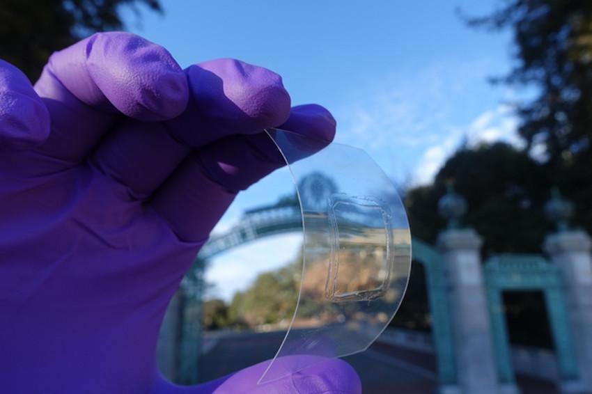 Applying mechanical strain on this atomically thin, transparent monolayer semiconductor results in a material with near 100 % light-emission efficiency. (Source: A. Javey, LBL)
The team identified just how the semiconductor’s electronic structure dictated interaction among the energetic particles within the material. Those particles sometimes collide and annihilate each other, losing energy as heat instead of emitting light in the process. Changing the material’s electronic structure reduced the likelihood for annihilation and led to a near-perfect conversion of energy to light, even at high brightness. “It’s always easier to emit heat than emit light, particularly at high brightness levels. In our work we have been able to reduce the loss process by one hundredfold,” said Ali Javey, professor of electrical engineering and computer sciences at UC Berkeley.
The Berkeley team’s discovery was made using a single, 3-atom-thick layer of a type of semiconductor material, a transition metal dichalcogenide, that was subjected to mechanical strain. These thin materials have a unique crystal structure that gives rise to unique electronic and optical properties: When their atoms are excited either by passing an electric current or shining light, excitons are created. Excitons can release their energy either by emitting light or heat. The efficiency with which excitons emit light as opposed to heat is an important metric that determines the ultimate performance of LEDs. But achieving high performance requires precisely the right conditions.
“When the exciton concentration is low, we had previously found how to achieve perfect light-emission efficiency,” said Shiekh Zia Uddin, a UC Berkeley graduate student. He and his colleagues had shown that chemically or electrostatically charging single-layered materials could lead to high-efficiency conversion, but only for a low concentration of excitons. For the high exciton concentration at which optical and electronic devices typically operate, though, too many excitons annihilate each other. The Berkeley team’s new work suggests that the trick to achieve high performance for high concentrations lay in tweaking the material’s band structure, an electronic property that controls how excitons interact with each other and could reduce the probability of exciton annihilation.
“When more excited particles are created, the balance tilts toward creating more heat instead of light. In our work, we first understood how this balance is controlled by the band structure,” said Hyungjin Kim, a postdoctoral fellow. That understanding led them to propose modifying the band structure in a controlled way using physical strain. The researchers started by carefully placing a thin semiconductor (tungsten disulfide, WS2) film atop a flexible plastic substrate. By bending the plastic substrate, they applied a small amount of strain to the film. At the same time, the researchers focused a laser beam with different intensities on the film, with a more intense beam leading to a higher concentration of excitons – a high brightness setting in an electronic device.
Detailed optical microscope measurements allowed the researchers to observe the number of photons emitted by the material as a fraction of the photons it had absorbed from the laser. They found that the material emitted light at nearly perfect efficiency at all brightness levels through appropriate strain. To further understand the material’s behavior under strain, the team performed analytical modelling. They found that the heat-losing collisions between excitons are enhanced due to saddle points – regions where an energy surface curves in a way that resembles a mountain pass between two peaks – found naturally in the single-layer semiconductor’s band structure.
Applying the mechanical strain led the energy of that process to change slightly, drawing the excitons away from the saddle points. As a result, the particles’ tendency to collide was reduced, and the reduction in efficiency at high concentrations of charged particles ceased to be a problem. “These single-layer semiconductor materials are intriguing for optoelectronic applications as they uniquely provide high efficiency even at high brightness levels and despite the presence of large number of imperfections in their crystals,” said Javey. Future work by the Berkeley Lab team will focus on using the material to fabricate actual LED devices for further testing of the technology’s high efficiency under increasing brightness. (Source: LBNL)
Reference: H. Kim et al.: Inhibited nonradiative decay at all exciton densities in monolayer semiconductors, Science 373, 448 (2021); DOI: 10.1126/science.abi9193