New device converts IR-light into images
07.05.2021 - An infrared imager combines the sensors and the display into one thin device.
Seeing through smog and fog. Mapping out a person's blood vessels while monitoring heart rate at the same time – without touching the person's skin. Seeing through silicon wafers to inspect the quality and composition of electronic boards. These are just some of the capabilities of a new infrared imager developed by a team of researchers led by electrical engineers at the University of California San Diego.
-
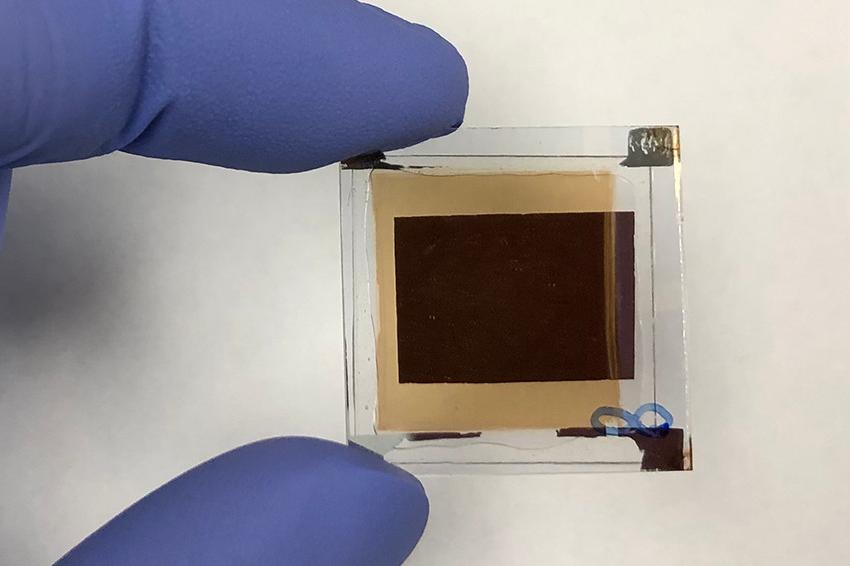 The new infrared imager is thin and compact with a large-area display. (Source: N. Li)
The imager detects shortwave infrared light, which is right outside of the visible spectrum. Shortwave infrared imaging is not to be confused with thermal imaging, which detects much longer infrared wavelengths given off by the body. The imager works by shining shortwave infrared light on an object or area of interest, and then converting the low energy infrared light that's reflected back to the device into shorter, higher-energy wavelengths that the human eye can see.
“It makes invisible light visible,” said Tina Ng, a professor of electrical and computer engineering at the UC San Diego Jacobs School of Engineering. While infrared imaging technology has been around for decades, most systems are expensive, bulky and complex, often requiring a separate camera and display. They are also typically made using inorganic semiconductors, which are costly, rigid and consist of toxic elements such as arsenic and lead.
The infrared imager that Ng's team developed overcomes these issues. It combines the sensors and the display into one thin device, making it compact and simple. It is built using organic semiconductors, so it is low cost, flexible and safe to use in biomedical applications. It also provides better image resolution than some of its inorganic counterparts.
The new imager offers additional advantages. It sees more of the shortwave infrared spectrum, from 1000 to 1400 nanometers – existing similar systems often only see below 1200 nanometers. It also has one of the largest display sizes of infrared imagers to date: 2 square centimeters in area. And because the imager is fabricated using thin film processes, it is easy and inexpensive to scale up to make even larger displays.
The imager is made up of multiple semiconducting layers, each hundreds of nanometers thin, stacked on top of one another. Three of these layers, each made of a different organic polymer, are the imager's key players: a photodetector layer, an organic light-emitting diode (OLED) display layer, and an electron-blocking layer in between. The photodetector layer absorbs shortwave infrared light and then generates an electric current. This current flows to the OLED display layer, where it gets converted into a visible image. An intermediate layer, called the electron-blocking layer, keeps the OLED display layer from losing any current. This is what enables the device to produce a clearer image.
This upconversion process is electronic. “The advantage of this is it allows direct infrared-to-visible conversion in one thin and compact system,” said Ning Li, a postdoctoral researcher in Ng's lab. “In a typical IR imaging system where upconversion is not electronic, you need a detector array to collect data, a computer to process that data, and a separate screen to display that data. This is why most existing systems are bulky and expensive.” Another special feature is that the imager is efficient at providing both optical and electronic readouts. “This makes it multifunctional,” said Li. For example, when the researchers shined infrared light on the back of a subject's hand, the imager provided a picture of the subject's blood vessels while recording the subject's heart rate.
The researchers also used their infrared imager to see through smog and a silicon wafer. In one demonstration, they placed a photomask patterned with “EXIT” in a small chamber filled with smog. In another, they placed a photomask patterned with “UCSD” behind a silicon wafer. Infrared light penetrates through both smog and silicon, making it possible for the imager to see the letters in these demonstrations. This would be useful for applications such as helping autonomous cars see in bad weather and inspecting silicon chips for defects. The researchers are now working on improving the imager's efficiency. (Source: UCSD)