New imaging method to assess quality of 3D-printed metal parts
Scientists from NTU Singapore have developed a fast imaging system to analyze the inner structure of 3D-printed metal parts.
Most 3D-printed metal alloys consist of a myriad of microscopic crystals, which differ in shape, size, and atomic lattice orientation. By mapping out this information, scientists and engineers can infer the alloy’s properties, such as strength and toughness. This is similar to looking at wood grain, where wood is strongest when the grain is continuous in the same direction. This new technology, made by researchers of the Nanyang Technological University, Singapore, could benefit the aerospace sector, where low-cost, rapid assessment of mission critical parts – turbine, fan blades and other components – could be a gamechanger for the maintenance, repair and overhaul industry.
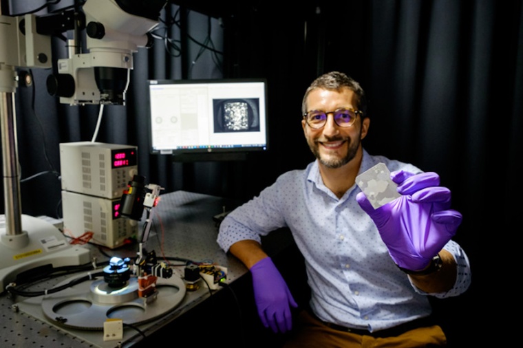
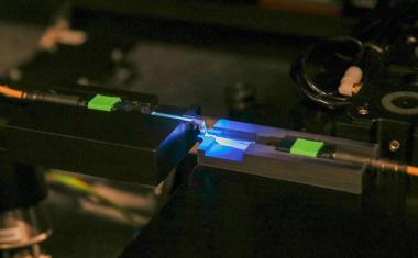
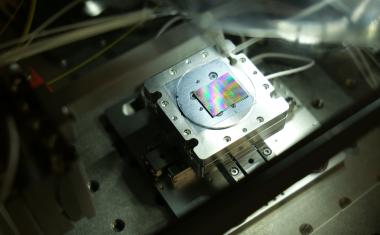
Until now, analyzing this microstructure in 3D printed metal alloys has been achieved through laborious and time-consuming measurements using scanning electron microscopes. The method designed by Matteo Seita and his team, provides the same quality of information in a matter of a minutes by using a system consisting of an optical camera, a flashlight, and a notebook computer that runs a proprietary machine-learning software developed by the team – with the hardware costing about S$ 25,000.
The team’s new method first requires treating the metal surface with chemicals to reveal the microstructure, then placing the sample facing the camera, and taking multiple optical images as the flashlight illuminates the metal from different directions. The software then analyses the patterns produced by light that is reflected off the surface of different metal crystals and deduces their orientation. The entire process takes about 15 minutes to complete.
“Using our inexpensive and fast-imaging method, we can easily tell good 3D-printed metal parts from the faulty ones. Currently, it is impossible to tell the difference unless we assess the material’s microstructure in detail,” explains Seita. “No two 3D-printed metal parts are created equal, even though they may have been produced using the same technique and have the same geometry. Conceptually, this is akin to how two otherwise identical wooden artefacts may each possess a different grain structure.”
Seita believes that their innovative imaging method has the potential to simplify the certification and quality assessment of metal alloy parts produced by 3D printing. One of the most commonly used techniques to 3D print metal parts uses a high-powered laser to melt metal powders and fuse them together, layer by layer, until the full product is printed. However, the microstructure and thus the quality of the resulting printed metal depends on several factors, including how fast or intense the laser is, how much time is given for the metal to cool before the next layer is melted, and even the type and brand of metal powders used.
This is why the same design printed by two different machines or production house may result in parts of different quality. Instead of using a complicated computer programme to measure the crystal orientation from the optical signals acquired, the smart software uses a neutral network. The team then used machine learning to programme the software, by feeding it hundreds of optical images. Eventually, their software learned how to predict the orientation of crystals in the metal from the images, based on differences in how light scatters off the metal surface. It was then tested to be able to create a complete crystal orientation map, which provides comprehensive information about the crystal shape, size, and atomic lattice orientation.
To commercialize their method, the team is now in discussion with NTUitive, NTU’s innovation and enterprise company, to explore the possibility of starting a spin-off company or to license their patent to interested industry players. (Source: NTU)