New nanocavities pave the way for enhanced tiny lasers and LEDs
26.01.2024 - Sub-wavelength confinement of light demonstrated in indium phosphide nanocavity could enable faster data transmission using smaller, more energy-efficient devices.
As industry transitions to a new era in computing, there is a need for new devices that integrate electronic and photonic functionalities at the nanoscale while enhancing the interaction between photons and electrons. In an important step toward fulfilling this need, researchers have developed a new III-V semiconductor nanocavity that confines light at levels below the so-called diffraction limit.
-
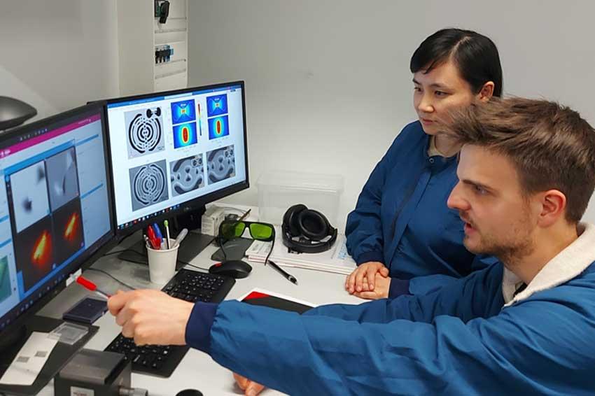 Meng Xiong and Frederik Schröder of the research team (Source: DTU)
 -
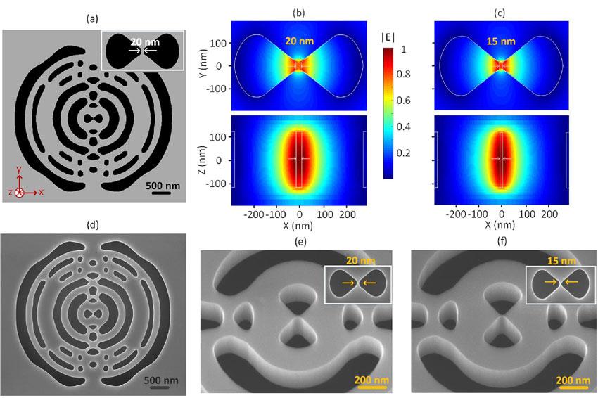 III-V semiconductor nanocavity that confines light at levels below the diffraction limit. The design of the cavity is shown in a, the calculated electric field distribution in b and c, and scanning electron microscopy images in d-f. (Source: Xiong et al., DTU / Optica)
“Nanocavities with ultrasmall mode volumes hold great promise for improving a wide range of photonic devices and technologies, from lasers and LEDs to quantum communication and sensing, while also opening up possibilities in emerging fields such as quantum computing,” said Meng Xiong from the Technical University of Denmark. “For example, light sources based on these nanocavities could significantly improve communication by enabling faster data transmission and strongly reduced energy consumption.”
The new nanocavity exhibits a mode volume an order of magnitude smaller than previously demonstrated in III-V materials. The strong spatial confinement of light demonstrated in this work helps enhance light-matter interaction, which allows higher LED powers, smaller laser thresholds and higher single-photon efficiencies.
“Light sources based on these new nanocavities could have a major impact on data centers and computers, where ohmic and power-hungry connections could be replaced by high-speed and low-energy optical links,” said Xiong. “They could also be used in advanced imaging techniques such as super-resolution microscopy to enable better disease detection and treatment monitoring or to improve sensors for various applications, including environmental monitoring, food safety and security.”
The work is part of an effort by researchers at the Technical University of Denmark’s NanoPhoton – Center for Nanophotonics who are exploring a new class of dielectric optical cavities that enable deep subwavelength confinement of light through a principle the researchers have coined extreme dielectric confinement (EDC). By enhancing the interaction between light and matter, EDC cavities could lead to highly efficient computers with deep-subwavelength lasers and photodetectors that are integrated into transistors for reduced energy consumption.
In the new work, the researchers first designed an EDC cavity in the III-V semiconductor indium phosphide (InP) using a systematic mathematical approach that optimized the topology while relaxing geometric constraints. They then fabricated the structure using electron beam lithography and dry etching.
“EDC nanocavities have feature sizes down to a few nanometers, which is crucial for achieving extreme light concentration, but they also come with a significant sensitivity to fabrication variations,” said Xiong. “We attribute successful realization of the cavity to the improved accuracy of the InP fabrication platform, which is based on electron beam lithography followed by dry etching.”
After refining the fabrication process, the researchers achieved a remarkably small dielectric feature size of 20 nm, which became the basis for the second round of topological optimization. This last round of optimization produced a nanocavity with a mode volume of just 0.26 (λ/2n)³, where λ represents the wavelength of light and n its refractive index. This achievement is four times smaller than what is often termed the diffraction-limited volume for a nanocavity, which corresponds to a box of light with a side-length of half the wavelength.
The researchers point out that although similar cavities with these characteristics were recently achieved in silicon, silicon lacks the direct band-to-band transitions found in III-V semiconductors, which are essential for harnessing the Purcell enhancement provided by nanocavities. “Prior to our work, it was uncertain whether similar outcomes could be achieved in III-V semiconductors because they don't benefit from the advanced fabrication techniques developed for the silicon electronics industry,” said Xiong.
The researchers are now working to improve the fabrication precision to further reduce the mode volume. They also want to use the EDC cavities to achieve a practical nanolaser or nanoLED.
Reference: M. Xiong, R. E. Christiansen, F. Schroder, Y. Yu, L. Nevenka Casses, E. Semenova, K. Yvind, N. Strenger, O. Sigmund, J. Mork: Experimental realization of deep sub-wavelength confinement of light in a topology-optimized InP nanocavity, Opt. Mater. Express 14(2), pp. 397-406 (2024); DOI: 10.1364/ome.513625
Link: Center for Nanophotonics, Technical University of Denmark (DTU), Kongens Lyngby, Denmark