New technology for laser glass wafer dicing from Corning
Corning has launched a dicing technology that will allow the company’s laser technologies business to enter the semiconductor application space to further focus on microfabrication processes.
Corning Laser Technologies (CLT) advanced its patented nanoperforation process and paired it with a well-established breaking technology from Dynatex International, an industry leader in mechanical breaking of crystalline wafers, to create a new glass wafer dicing technology.
The new technology will allow customers to drive lower cost through significantly higher throughput as well as achieve lower, near-zero kerf loss and high edge strength through an inherently clean process that will eliminate subsequent cleaning steps.
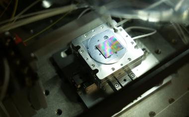
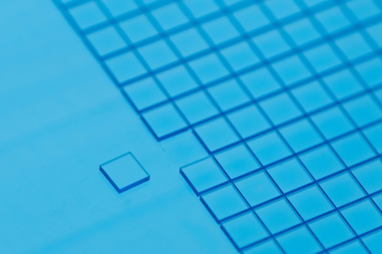
Additionally, the glass wafer dicing technology for up to 300 mm diameter glass wafers achieves superior results on yield, enabling unprecedented die aspect ratios and a sidewall quality that meets the highest demands of the semiconductor industry. The innovation was developed for use in industries such as microfluidics and micro-optics. It can also be applied for meta-surfaces on glass and other glass wafer-based semiconductor applications, as well as dicing of other brittle and transparent materials.
“We are looking forward to leveraging our 20-plus years of experience in precision laser machining along with Dynatex’s expertise in breaking tools and supporting equipment,” said Michael Mueller, business director, Precision Glass Solutions and Corning Laser Technologies. “This novel wafer dicing method will help Corning continue to grow in the semiconductor industry and innovate to meet current and future demands.”
With decreasing die sizes and increasing wafer diameters, material utilization becomes significantly more important for high-yield semiconductor applications. When comparing to a kerf-removing technology such as blade dicing (calculated with a kerf loss of 0.2 mm), CLT’s new laser dicing method can increase utilization of a wafer with small dies of 5 × 5 mm by 8 % and even smaller dies of 2 × 2 mm by 17 %. Enabled by the near-zero kerf loss, a fully populated 300 mm diameter and 0.7 mm thick wafer can provide a wafer utilization of 96 % calculated with an edge exclusion of 5 mm.
Small dies on large glass wafers require a high-quality and high-speed dicing process. With the die size of 5 × 5 mm, a 300 mm wafer can be fully diced in less than ten minutes – significantly faster than classical blade dicing, which requires multiple hours to cut.
Additionally, when using Corning HPFS fused silica, a semiconductor-ready wafer material known for its high transparency, results demonstrate the exceptional performance for chipping and edge quality. HPFS wafers allow for low chipping that is better than 50 µm with very precise edges and die corners.
Further reading: Julia Brueckner, Andreas Gaab, and Prakash Gajendran (all: Corning): Combining High-Tech Glass Innovations with Advanced Laser Technologies – High-quality glass substrates and supporting laser capabilities for semiconductor and microelectronics applications, PhotonicsViews 17(5), October/November 2020; DOI: 10.1002/phvs.202000037