Joint development of data storage on 300 mm wafers
16.05.2025 - NY Creates and Fraunhofer IPMS will work together to develop and characterize devices that are critical to advancing the portfolios of both organizations.
At a ceremony, the New York Center for Research, Economic Advancement, Technology, Engineering, and Science, NY Creates, and the Fraunhofer Institute for Photonic Microsystems signed a new joint development agreement to advance research and development in the field of data storage.
-
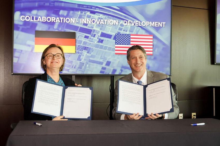 Dr Wenke Weinreich (l), deputy director of Fraunhofer IPMS, and NY Creates VP and COO Paul Kelly (Source: NY Creates)
“We are building on the strong relationships we have with semiconductor research and development organizations around the world to create technologies that the U.S. and the world will depend on in the future. So we look forward to this collaboration with Fraunhofer IPMS to further develop the next generation of ferroelectric memory devices on 300 mm wafers,” said Dave Anderson, president of NY Creates.
Dr Wenke Weinreich, Deputy Director of Fraunhofer IPMS, added: “With the Center Nanoelectronic Technologies (CNT), Fraunhofer IPMS operates a leading international competence center for the development of ferroelectric memories based on hafnium oxide (HfO2). These memory technologies are particularly promising for neuromorphic computing as they are very energy efficient, CMOS compatible and scalable down to very small technology nodes. We look forward to working with NY Creates to develop promising new memory designs based on the expertise of both parties.”
Senior members of NY Creates, based in Albany, New York, and Dresden-based Fraunhofer IPMS sealed the JDA on May 15 at NY Creates’ Albany NanoTech Complex with a signing ceremony by Paul Kelly, vice president of strategies, partnerships, and new ventures, and chief operating officer of NY Creates, and Dr Wenke Weinreich, deputy director of Fraunhofer IPMS, in the presence of numerous high-level representatives from New York State and Germany. Based on this agreement, NY Creates and Fraunhofer IPMS are launching a joint development project for the development of advanced data storage on 300 mm wafers, the current industry standard for chip manufacturing.
Contact
Fraunhofer Institut für Photonische Mikrosysteme IPMS
Maria-Reiche-Str. 2
01109 Dresden
Germany
+49 351 8823-0
+49 351 8823-266