Leaky-wave metasurfaces
A perfect interface between free-space and integrated optical systems.
Researchers at Columbia Engineering have developed a new class of integrated photonic devices – leaky-wave metasurfaces – that can convert light initially confined in an optical waveguide to an arbitrary optical pattern in free space. These devices are the first to demonstrate simultaneous control of all four optical degrees of freedom, namely, amplitude, phase, polarization ellipticity, and polarization orientation. Because the devices are so thin, transparent, and compatible with photonic integrated circuits (PICs), they can be used to improve optical displays, Lidar, optical communications, and quantum optics.
“We are excited to find an elegant solution for interfacing free-space optics and integrated photonics – these two platforms have traditionally been studied by investigators from different subfields of optics and have led to commercial products addressing completely different needs,” said Nanfang Yu, researcher on nanophotonic devices. “Our work points to new ways to create hybrid systems that utilize the best of both worlds – free-space optics for shaping the wavefront of light and integrated photonics for optical data processing – to address many emerging applications such as quantum optics, optogenetics, sensor networks, inter-chip communications, and holographic displays.”
The key challenge of interfacing PICs and free-space optics is to transform a simple waveguide mode confined within a waveguide into a broad free-space wave with a complex wavefront, and vice versa. Yu’s team tackled this challenge by building on their invention last fall of nonlocal metasurfaces and extended the devices’ functionality from controlling free-space light waves to controlling guided waves. Specifically, they expanded the input waveguide mode by using a waveguide taper into a slab waveguide mode – a sheet of light propagating along the chip.
“We realized that the slab waveguide mode can be decomposed into two orthogonal standing waves,” said Heqing Huang, a PhD student in Yu’s lab. “Therefore, we designed a leaky-wave metasurface composed of two sets of rectangular apertures that have a subwavelength offset from each other to independently control these two standing waves. The result is that each standing wave is converted into a surface emission with independent amplitude and polarization; together, the two surface emission components merge into a single free-space wave with completely controllable amplitude, phase, and polarization at each point over its wavefront.”
Yu’s team experimentally demonstrated multiple leaky-wave metasurfaces that can convert a waveguide mode propagating along a waveguide with a cross-section on the order of one wavelength into free-space emission with a designer wavefront over an area about 300 times the wavelength at the telecom wavelength of 1.55 microns. These include: A leaky-wave metalens that produces a focal spot in free space. Such a device will be ideal for forming a low-loss, high-capacity free-space optical link between PIC chips; it will also be useful for an integrated optogenetic probe that produces focused beams to optically stimulate neurons located far away from the probe.
In addition: a leaky-wave optical-lattice generator that can produce hundreds of focal spots forming a Kagome lattice pattern in free space. In general, the leaky-wave metasurface can produce complex aperiodic and three-dimensional optical lattices to trap cold atoms and molecules. This capability will enable researchers to study exotic quantum optical phenomena or conduct quantum simulations hitherto not easily attainable with other platforms, and enable them to substantially reduce the complexity, volume, and cost of atomic-array-based quantum devices. For example, the leaky-wave metasurface could be directly integrated into the vacuum chamber to simplify the optical system, making portable quantum optics applications, such as atomic clocks, a possibility.
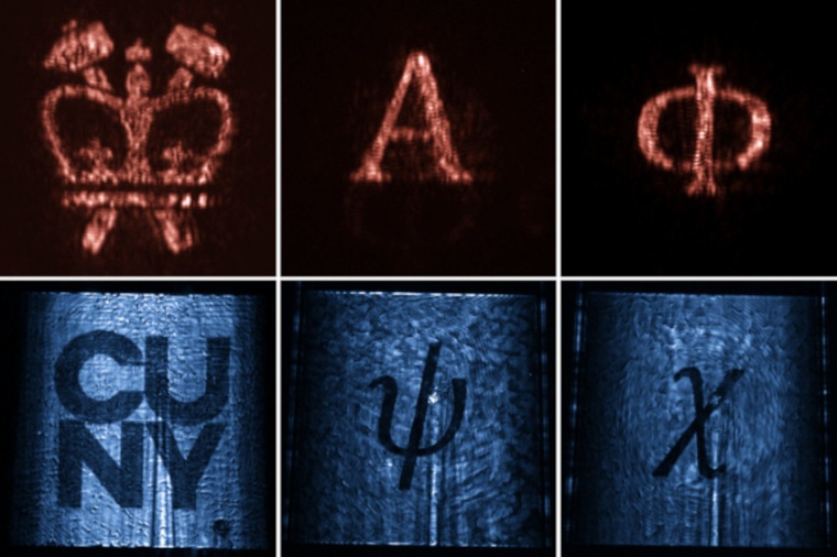
A leaky-wave vortex-beam generator that produces a beam with a corkscrew-shaped wavefront could lead to a free-space optical link between buildings that relies on PICs to process information carried by light, while also using light waves with shaped wavefronts for high-capacity intercommunication. A leaky-wave hologram that can displace four distinct images simultaneously: two at the device plane (at two orthogonal polarization states) and another two at a distance in the free space (also at two orthogonal polarization states). This function could be used to make lighter, more comfortable augmented reality goggles and more realistic holographic 3D displays.
Yu’s current demonstration is based on a simple polymer-silicon nitride materials platform at near-infrared wavelengths. His team plans next to demonstrate devices based on the more robust silicon nitride platform, which is compatible with foundry fabrication protocols and tolerant to high optical power operation. They also plan to demonstrate designs for high output efficiency and operation at visible wavelengths, which is more suitable for applications such as quantum optics and holographic displays. (Source: CUNY)
Link: Dept. of Applied Physics and Applied Mathematics (N. Yu), Columbia University, New York, USA