No computer Chips without Industrial Image Processing
Machine vision technologies contribute to a high level of quality in all process steps of semiconductor manufacturing. Which concrete application scenarios of industrial image processing are conceivable in the production and inspection of semiconductors and what relevance does the software have in this context?
The semiconductor industry is constantly facing new challenges due to volatile market conditions. In addition, the demand for corresponding components is increasing continuously and at a high pace. With the increasing digitalization of the economy and society, the components are needed for many different products. In addition to industry, the consumer electronics sector with a wide variety of applications such as entertainment and e-mobility also demands semiconductors. The increased connection of home workstations to company networks has also led to a run on semiconductor components.
In addition, during the Covid 19 pandemic, the global flow of goods and supply chains in the semiconductor industry are undergoing profound changes. This has a lasting impact, as this industry in particular places high demands on quality and precision in the manufacturing and inspection process. In addition, the pressure for automation is growing due to rapidly increasing labor costs. And last but not least, as in most technically oriented industries, there is a shortage of qualified personnel. For all these reasons, manufacturers of semiconductor components are forced to optimize their value creation processes and to adapt production capacities quickly and flexibly to changing conditions.
Machine vision enables high degree of automation
Machine vision, i.e. industrial image processing, offers the potential to master precisely these challenges quickly and efficiently. Corresponding applications are already making a valuable contribution to the end-to-end networking and digitization of production processes in the sense of Industry 4.0 and Smart Factory - from manufacturing to quality assurance to logistical workflows.
Machine vision enables robust detection rates and thus a high degree of automation in assembly and inspection. Moreover, machine vision is already integrated in all conceivable production environments, can be used around the clock as well as independently of human working hours, and is superior to human colleagues in terms of reliability in inspection activities.
Matching methods are most frequently used in semiconductor production. The position of objects can be determined with an accuracy of up to 1/20 pixel in the image, allowing them to be precisely aligned. Other elementary applications are measuring, OCR, i.e. text recognition, and quality inspection during welding.
Multiple process steps in semiconductor manufacturing
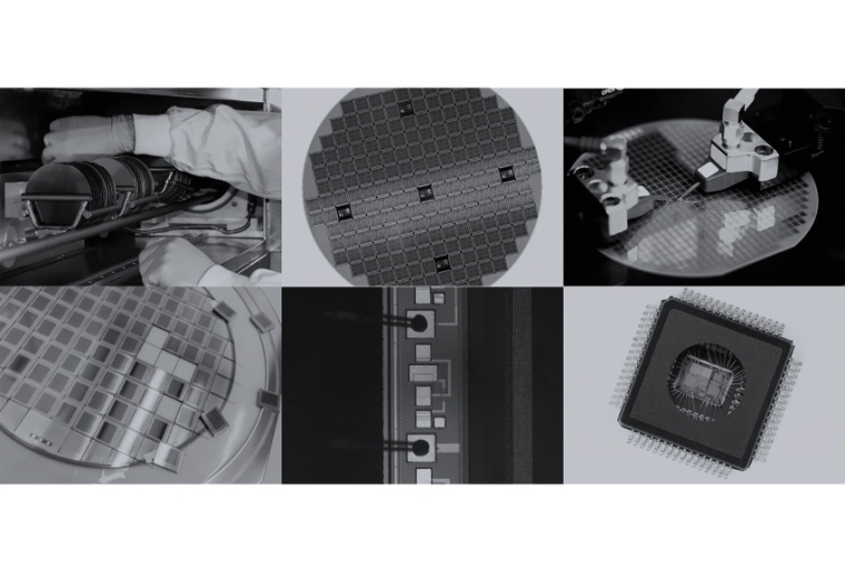
Semiconductor production is characterized by complex workflows and comprises more than 1,000 different process steps. Essentially, production is made up of three phases:
- the wafer production,
- the front-end and
- the back-end process.
In turn, wafer processing is divided into several individual steps. These include:
- the cutting of the cast blocks into wafers,
- the sorting, polishing and etching of the circuits,
- testing by probers,
- the cutting,
- ball and wire bonding, and
- packaging.
In almost all process steps, machine vision can support and significantly improve the results. This is especially true for quality control, which plays a special role in wafer processing. The speed and precision requirements here are very high. For example, accuracies in the micrometer range (My) must be maintained here in order to guarantee the quality of the components. Therefore, it is necessary to monitor all production steps in a very detailed and seamless manner. A wide range of inspection tasks can be solved with image processing.
Alignment of wafers using image processing
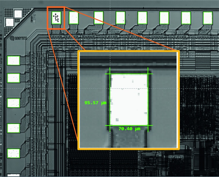
Matching plays the most important role in the quality assurance process. One example is prober testing. This involves the alignment of the wafers. Even small positioning errors can cause the prober needle, for example, to miss its target and destroy the chip. For positioning, the dies, i.e. the individual chips on the wafer, are precisely located on the opposite sides of the wafer using shape matching and the necessary position correction is calculated.
Another example of a process in which matching methods are used is the cutting of wafers. This involves preparing machines for further processing of the wafers. The challenge is to determine the orientation and position of the wafer. Here, a machine vision process is used to determine the center of rotation, from which the exact alignment can finally be determined. Subsequently, edge detection algorithms and filters help to measure the individual chips on the wafer with high precision in order to determine the optimum cutting edges.
Determining the position of the chip in the package
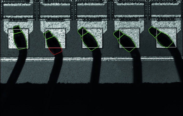
Once the individual chips have been cut from the wafer, they are inserted into the electronic component in the next process step. Here, position determination is an important element in quality control. In concrete terms, for example, it is a matter of determining the position of the chip relative to the package after it has been inserted into the electronic component. This is important for the subsequent wire bonding, which creates the electronic connection between the chip and the component.
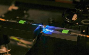
Different quality inspection tasks are used during wire bonding. For some chip types, for example, the height of the wires must be inspected. Other inspections are used to detect defects. Defects can include incorrect position, incorrect cut length and incorrect pressure during bonding. Machine vision technologies are used here to extract the contact points (pads) and wires and narrow down the relevant areas. These are then analyzed for alignment and overlap to ensure correct bonding.
Other elementary technologies include identification processes such as optical character recognition (OCR). These enable the precise reading of number combinations and thus the recognition of the components. Wafers, for example, are marked with a lot number engraved by a laser. ECC200 codes (a variant of data matrix codes) can also be read uniquely to track each chip. These ID numbers can be used to identify each wafer on the production line.
Combining machine vision tools flexibly and easily
The machine vision standard software Halcon from MVTec Software, for example, offers a comprehensive toolbox that provides a wide range of useful functions for automated inspection processes in semiconductor manufacturing. These include surface inspection, shape matching, defect detection, completeness checking, alignment, deep learning, 2D and 3D object and position detection, 2D and 3D measurement, 3D vision, barcode and datacode reading, and OCR.
The image processing software can also be used for many other process steps in semiconductor manufacturing, such as testing wafers with probers, cutting wafers or ball and wire bonding. The particular advantage of Halcon is its range of functions, which can be used to solve a diverse spectrum of tasks in semiconductor production. In addition, it is possible to combine tools and operators seamlessly, flexibly and easily. This results in individual solutions that cover the respective quality management requirements in the industry one-to-one.
Author
Mario Bohnacker, Technical Product Manager Halcon at MVTec Software
Company
MVTec Software GmbHArnulfstraße 205
80634 München
Germany


most read

It Does Not Always Have to Be a Humanoid Robot
Mythomorphic design adds a distinct perspective to social robotics. Inspired by myths and fantasy rather than humans or animals, the article classifies examples and examines related opportunities and risks.
Precise Down to the Nanometer
Interferometry is crucial in semiconductor, packaging, and medical industries. New white‑light systems offer nanometer precision, high measurement rates, and are ideal for inline industrial use.
3D laser scanning for 100 percent inspection
Modern production requires precise, fast, and fully automated inspection processes. The robot-assisted inline measurement system Flexscan meets this requirement with two 3D compact sensors
The Rise of Photonic and Neuromorphic Computing: A New Era for AI Hardware
Computer Architectures for future data processing
Active Alignment in Assembly and Connection Technology
Reliable manufacturing processes are essential for the assembly and interconnection technology of photonics and optoelectronics systems.