Smart optics with nanostructures for cost-effective light management
Optics with multifunctional nanostructures for light guidance and scattering.
Lighting accounts for around one fifth of global energy consumption. Whether in soccer stadiums, public and private buildings, or vehicles, smart, cost-effective light management systems that detect and respond to lighting needs are in demand. In such systems, light-directing optics are used that have complex, three-dimensional surface structures. A team at the Fraunhofer Institute for Production Technology IPT in Aachen has now developed a new process that makes the production of light management optics much more cost-effective. The process can also be used in microfluidics and to produce antibacterial surfaces in the future.
A good light management system emits light only where it is actually needed and at the same time also controls the lighting intensity. The optics of such systems must direct and scatter the light as needed. For this purpose, the optics surfaces are usually provided with nanostructures that guide the light in the desired way. Various methods are used for structuring, for example etching processes, laser-based technologies or replicative processes such as injection molding or the modern and highly efficient process of precision molding, which can be used to produce high volumes in a short time. Another method is the lithographic structuring of individual optics using a laser.
In the ‘Intense’ research project, a team from the Fraunhofer IPT worked with project partners Temicon, Aixtooling, Micro Resist Technology, Holoeye Photonics, and Trilux, to develop a new process for manufacturing optics with such nanostructures for use in light management systems. The result at the end of the project was complex nanostructures that can perform several functions at once, such as scattering with simultaneous steering. Injection molding also allows the optics to be manufactured cost-effectively and in series.
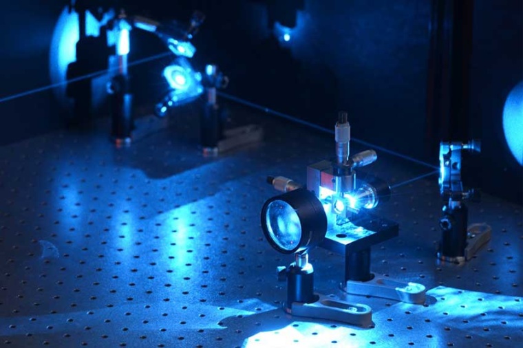
The researchers proceeded in three steps: First, they created a digital nanostructure template using a simulation program. Using an algorithm developed further at the IPT, they translated this digital master structure into a so-called phase image. In the third step, they used a spatial light modulator (SLM) to create a real 3D structure based on this phase image.
An SLM is a special type of interference lithography. Both transfer a 3D phase image into real three-dimensional structures by splitting a laser beam and superimposing the beams. However, in interference lithography, the laser beam is split only a few times, which makes it possible to create primarily periodic structures with structure sizes down to one hundred nanometers.
While in interference lithography only a few phase images can be realized, the SLM can generate an almost arbitrary phase image due to the large number of pixels, i.e. the laser is split millions of times depending on the complexity of the image. The superposition of these many partial beams provides a high-resolution image that can be used to create even highly complex three-dimensional structures. Both processes have the advantage that entire wafers can be structured at once. This can significantly speed up production and save costs.
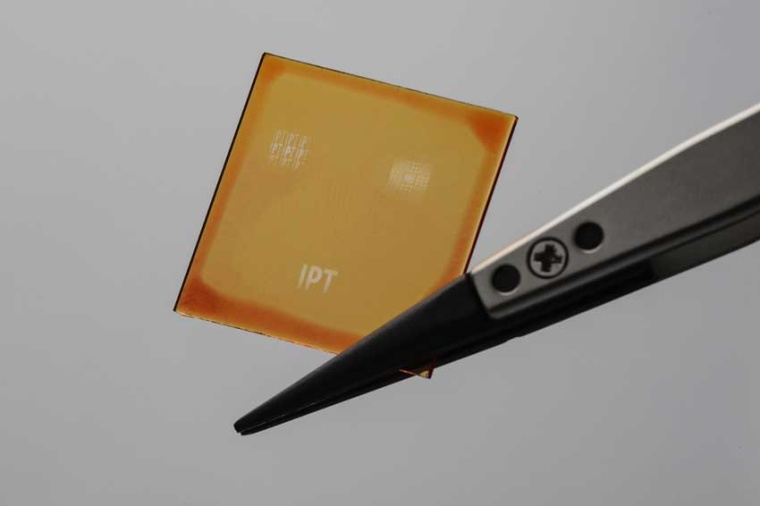
The phase image is transferred into real three-dimensional structures by introducing it into the surface of a polymer using SLM. In their test environment, the researchers structured surfaces ranging in size from one square millimeter to one square decimeter.
The result was surfaces with combined nanostructures that can now be used for molding in injection molding or the. Precision molding. “By combining the blaze grating and diffuser, we were able to achieve a combination of light-manipulating properties,” says project manager Cornelia Rojacher. “This means that multifunctional surfaces can now be created for the first time with just one manufacturing step.”
The researchers were also able to successfully test the combination of SLM and classical interference lithography. “The combination of the processes is interesting because in this way both the small feature sizes of interference lithography and the shape flexibility of SLM can be used simultaneously,” explains Rojacher.
Following the positive results, the researchers plan to further optimize the use of SLM for optics manufacturing. After all, with an even higher resolution, the technology will also become interesting for biological applications, such as the production of anti-bacterial or microfluidic structures. Reduced shape deviation should make the structures even smaller and more true to form. Another goal is to map the process onto curved surfaces as well, for example to produce cell scaffolds for the differentiation of stem cells.
Link: Research project "INTENSE", Fraunhofer Institute for Production Technology IPT, Aachen, Germany
Company
Fraunhofer-Institut für Produktionstechnologie IPTSteinbachstr. 17
52074 Aachen
Germany


most read
Ziehl-Abegg achieves sales of over one billion euros
This corresponds to growth of over 12% compared to the previous year. The global workforce increased from 5,300 to 5,800 employees.

Machine Safety 2026: The Five Most Important Trends for Eutomation Engineers
Digitalization and automation continue to drive mechanical engineering forward - and with them, the requirements for functional safety and cyber security are increasing. For automation engineers, this means that machine safety is becoming a holistic concept.

Spherea acquires Averna
The Spherea Group has signed an agreement to fully acquire the Canadian company Averna.

Hoerbiger takes over Physik Instrumente
With 1,900 employees, PI will form the new Positioning Division at Hoerbiger as an independent unit.
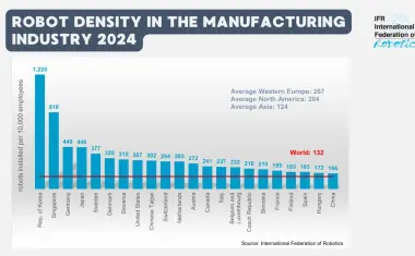
Global robot density: Western Europe leads ahead of North America and Asia
In the EU-27, the robot density is 231, which is above the global average of 132.